
All-metal three-dimensional circuits and memories

a three-dimensional circuit and memory technology, applied in the field of all-metal three-dimensional circuits and memories, can solve the problems of reducing the efficiency of semiconductor devices,

Active Publication Date: 2006-01-31
INTEGRATED MAGNETOELECTRONICS CO
View PDF50 Cites 26 Cited by
  • Summary
  • Abstract
  • Description
  • Claims
  • Application Information

AI Technical Summary

Benefits of technology

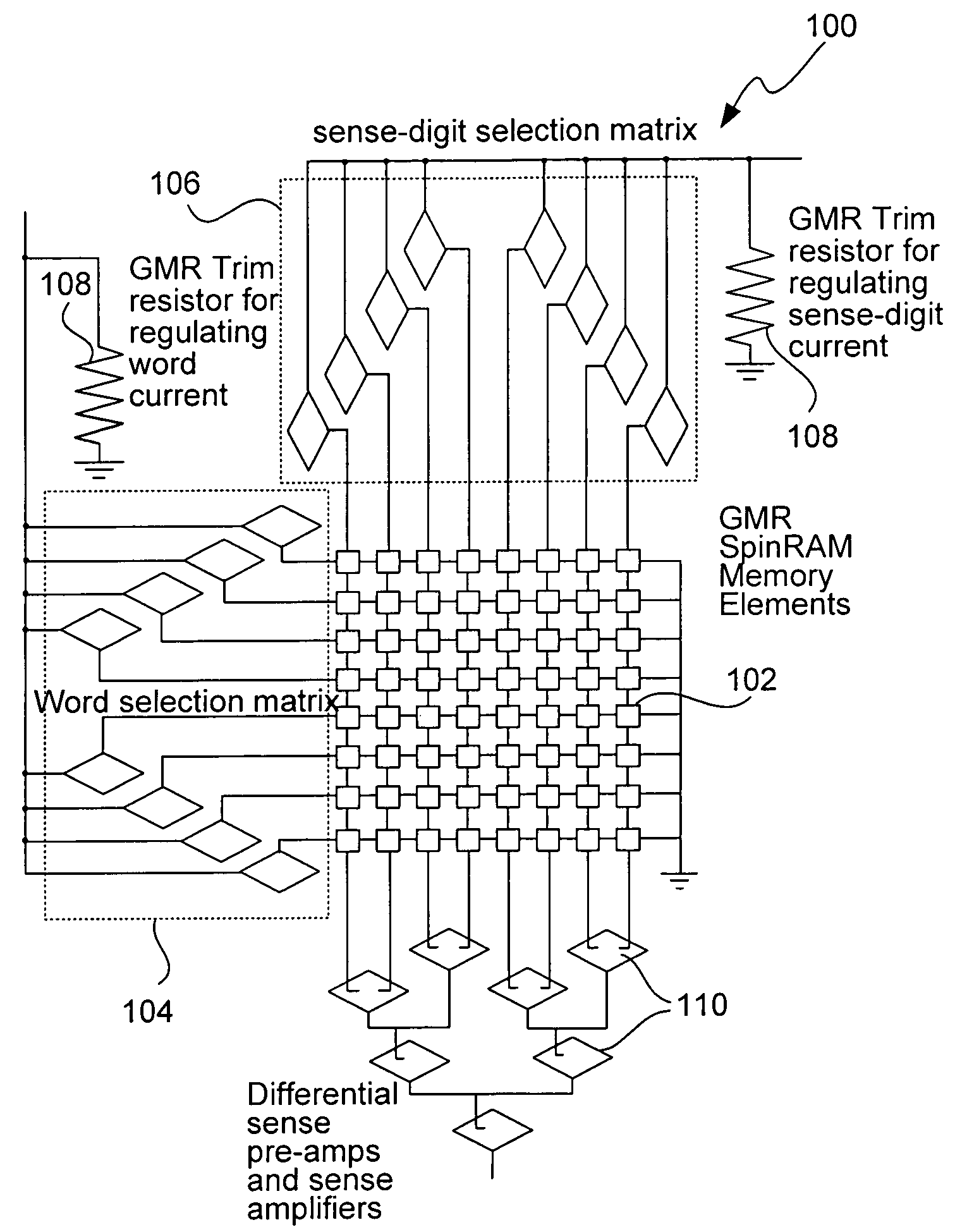
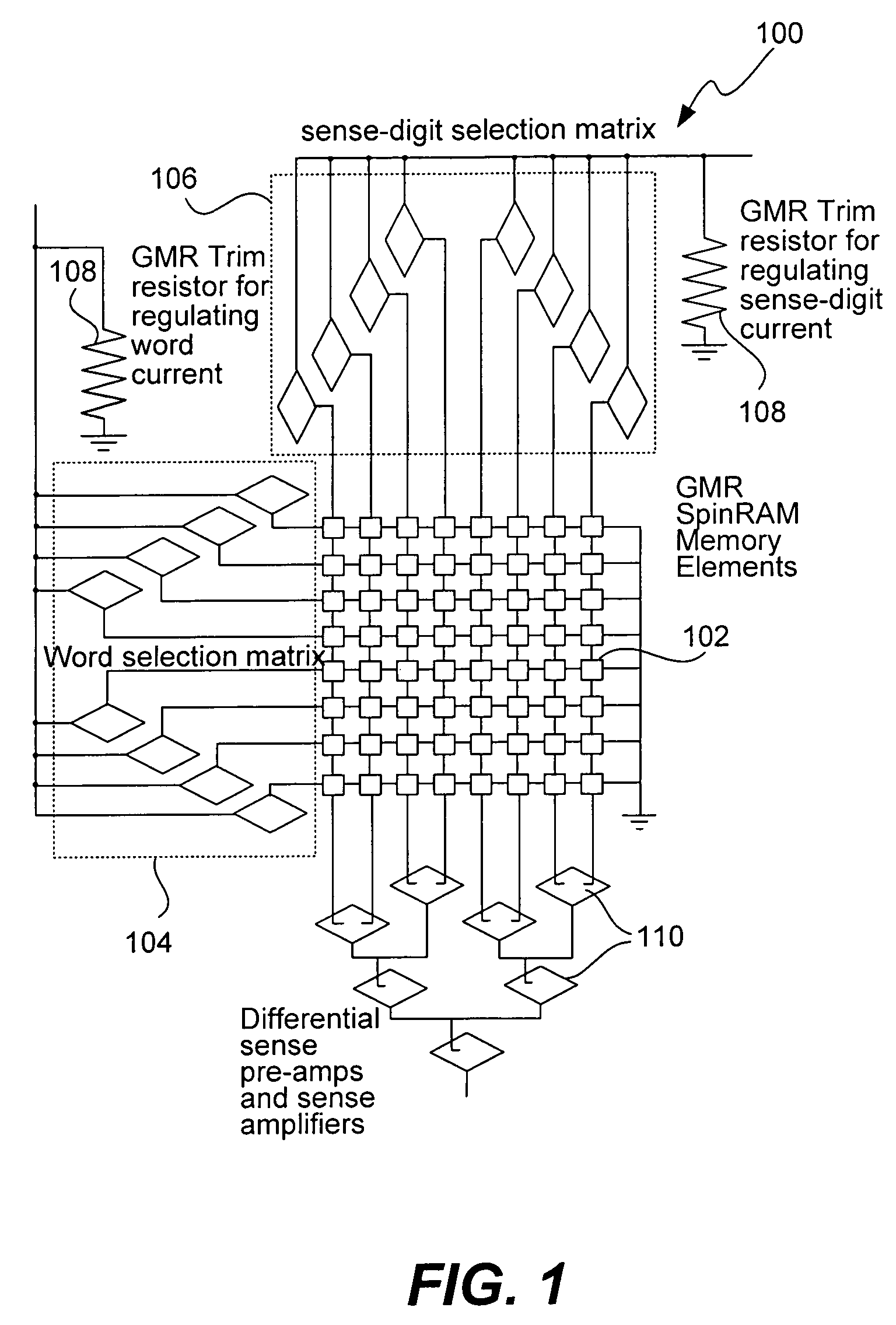
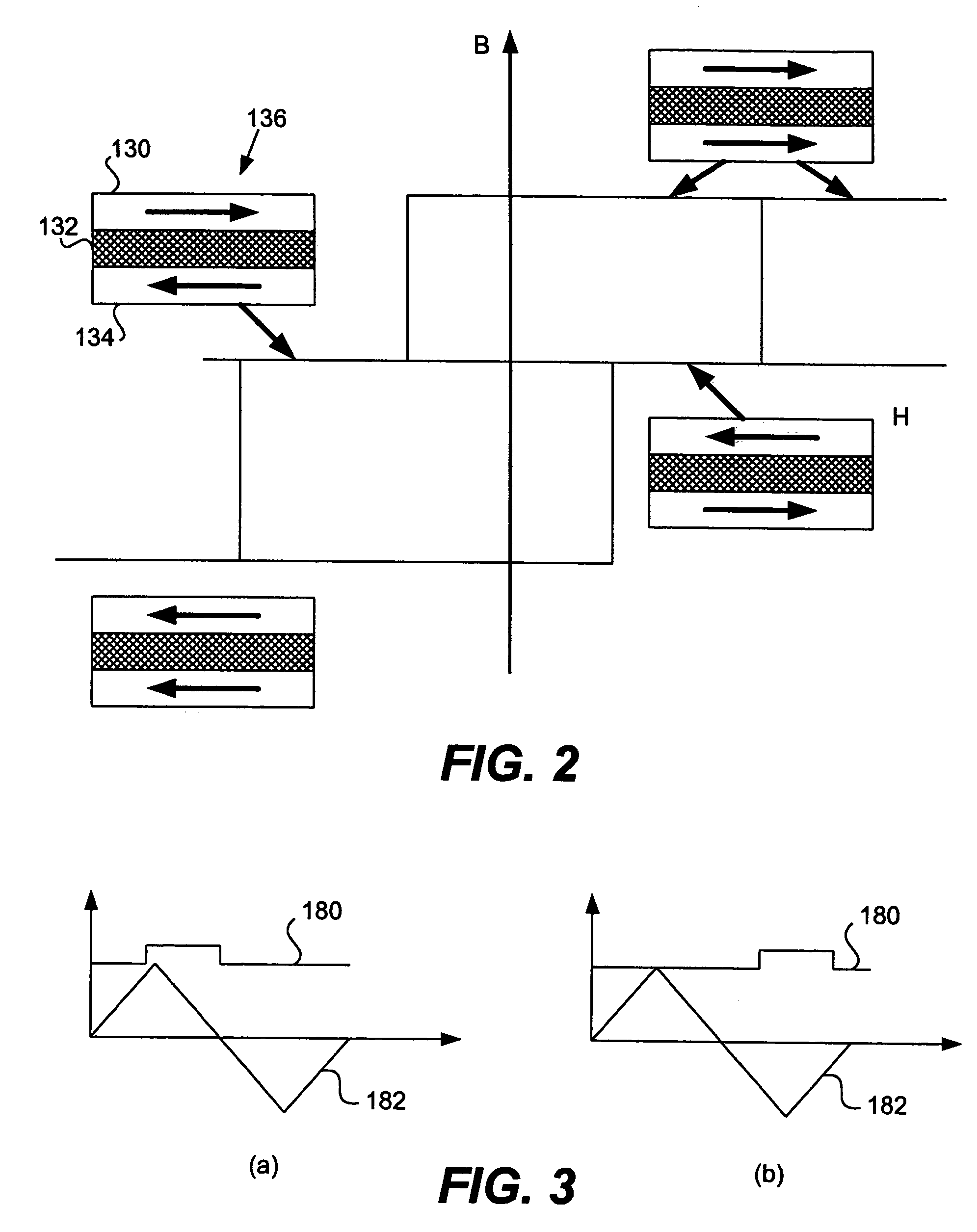
[0011]According to a more specific embodiment, the plurality of circuit components on at least one of the levels includes a plurality of memory cells. Each memory cell comprises a multi-layer structure exhibiting magnetoresistance. According to an even more specific embodiment, each multi-layer structure comprises a plurality of magnetic layers, at least one of which is operable to magnetically store one bit of information. A plurality of the access lines are integrated with the plurality of magnetic layers and are configured such that the bit of information may be accessed using selected ones of the plurality of access lines and the giant magnetoresistive effect. The multi-layer structure may also include at least one keeper layer. The magnetic layers and the access lines (with or without the keeper layer) are part of a substantially closed flux structure.
[0012]According to another specific embodiment, the plurality of circuit components on at least one of the levels includes a plurality of active circuit components. Each active circuit component is operable to generate an output signal based on the giant magnetoresistive effect. According to a more specific embodiment, at least one of the active circuit components is a transpinnor comprising a network of multi-layer thin-film elements, at least one of which exhibits giant magnetoresistance. The transpinnor further includes a conductor magnetically (i.e., not electrically or resistively) coupled to the at least one thin-film element for controlling operation of the transpinnor. The transpinnor is operable to generate an output signal which is a function of a resistive imbalance among the thin-film elements and which is proportional to a power current in the network of thin-film elements.

Problems solved by technology

The limitations of semiconductor technology are readily apparent in the widening gap between its future potential and its past performance.
In spite of the fact that the finer manufacturing geometry is aimed at offsetting the area increase brought about by the doubling of the transistor number, in practical terms the increase in number of transistors has increased the silicon area and the manufacturing costs.
Attempts to deposit silicon atoms, organized in perfect crystalline patterns, on top of an oxide, metal layer, or other layers have been unsuccessful thus far.
In addition, improvements in transistor performance are limited by physical and process technology constraints.
For example, as the feature size of silicon devices shrinks, undesirable effects occur including the loss of information through charge leakage, high oxide breakdown, and power consumption problems.
Inherent limitations such as the non-scalability of p-n junctions and charge pumps also translates into an inability to take full advantage of advances in lithography.
Memory systems which incorporate mechanical elements, e.g., disk drives, are also facing technological obstacles relating to storage density such as, for example, the difficulty of mechanically aligning a read head with increasingly smaller storage locations on a magnetic storage medium.
Such memories are also vulnerable to a variety of environmental stresses including, for example, shock, vibration, temperature extremes, radiation, etc.
In combination, such limitations impede the dual objectives of greater information density and faster information access.
However, these “hardcard” technologies do not have sufficient storage density or capacity to support the average stand-alone or networked computer system.
Indeed, with a fraction of the capacity of standard disks, FLASH and EEPROM provide only supplemental storage capacity and have the added disadvantage of a limited number of access cycles.
Moreover, although FLASH and EEPROM access times are better than those of conventional mechanical systems, they are clearly inferior as compared to DRAM or SRAM access times. In addition, the high power consumption per megabyte associated with FLASH and EEPROM necessitates larger power supplies, obviating the hardcard technologies' advantage in size and weight.
Therefore, although FLASH and EEPROM provide advantages with regard to speed and reliability, these memory technologies cannot achieve the capacity or endurance of conventional magnetic disk drives.

Method used


Image

  • All-metal three-dimensional circuits and memories
  • All-metal three-dimensional circuits and memories
  • All-metal three-dimensional circuits and memories

Examples


first embodiment

[0080] memory cell 702 becomes a four-bit memory cell with the addition of another access line (placed, for example, above cobalt layer 1) to break the symmetry which results in the interdependency of layers 704 and 710. This embodiment requires an additional masking level and an additional selection matrix to control the added access lines.

second embodiment

[0081] the compositions of storage layers 704 and 710 are made sufficiently different such that their switching thresholds require different field strengths for switching. This may be accomplished, for example, by depositing a permalloy layer directly over the cobalt film of storage layer 704. This will give layer 704 a lower coercivity than layer 710. Thus, when coincident currents are applied to the access lines, the resulting fields will write layer 704 before writing layer 710.

third embodiment

[0082] the separation spacing between the keepers and the cobalt storage films is adjusted such that demagnetizing fields become significant enough to break the symmetry. This embodiment takes advantage of the fact that even a perfect keeper doesn't completely cancel the demagnetizing field of a finite size magnetic film spaced a nonzero distance from the keeper. Such a demagnetizing field is proportional to the distance between the magnetic filed and the keeper. This demagnetizing field can be used to break the symmetry and allow both layer 704 and layer 710 to be written to the same state. For example, if one wishes to write a “0” to both layers 704 and 710, a pulse combination may first be applied which writes a “1” to layer 704 and a “0” to layer 710. A “1” is then written into each of layers 706 and 708. This results in a demagnetizing field which tends to bias layers 704 and 710 toward the “0” state. Thus, when a subsequent pulse combination is applied which tends to write lay...


PUM


Abstract

A three-dimensional circuit and methods for fabricating such a circuit are described. The three-dimensional circuit includes a plurality of stacked levels on a substrate. Each level includes a plurality of all-metal circuit components exhibiting giant magnetoresistance and arranged in two dimensions, the circuit further includes an interconnect for providing interconnections between the circuit components on different ones of the plurality of levels.

Description

RELATED APPLICATION DATA[0001]The present application claims priority from U.S. Provisional Patent Application No. 60 / 436,103 for MANUFACTURING OF 3D ELECTRONIC COMPONENTS AND OF 3D NONVOLATILE MEMORY COMPONENTS filed on Dec. 20, 2002, the entire disclosure of which is incorporated herein by reference for all purposes.BACKGROUND OF THE INVENTION[0002]The present invention relates to electronic systems and, more specifically, to electronic and data processing systems constructed using all-metal circuit components. Still more specifically, the present invention provides techniques for constructing all-metal, three-dimensional circuits in which circuit components are stacked on top of one another.[0003]Semiconductor technology provides the foundation of practically all electronic systems. The device density of silicon technology has increased steadily in the decades since its introduction and, until recently, roughly conformed to Moore's law which states that the device density of sili...

Claims


Application Information

Patent Timeline
Patent Type & Authority Patents(United States)
IPC IPC(8): G11C11/00G11C11/15
CPCG11C11/15
Inventor ANDREI, RADUSPITZER, RICHARDTOROK, E. JAMES
Owner INTEGRATED MAGNETOELECTRONICS CO
Learn More