Spin-injection magnetoresistance effect element

a technology of magnetoresistance and effect element, which is applied in the manufacture of flux-sensitive heads, instruments, record information storage, etc., can solve the problems of increasing the reversal time period, lowering the thermal fluctuation resistance, and complicated multi-layer structure of magnetic elements, and achieves high capacity, high speed, and low power consumption.

Inactive Publication Date: 2010-12-28
SONY CORP
View PDF3 Cites 19 Cited by
  • Summary
  • Abstract
  • Description
  • Claims
  • Application Information

AI Technical Summary

Benefits of technology

[0012]An object of the present invention therefore is to provide a spin-injection magnetoresistance effect element that can eliminate a conventional problem that the critical current Ic of spin-injection magnetization reversal has a high current value on the order of several hundred microamperes to several milliamperes, and allows use of a large reading current.
[0019]Examples of material of the first nonmagnetic film in a multi-layer structure with a TMR effect include the following substances: aluminum oxides (AlOx); an aluminum nitride (AlN), a magnesium oxide (MgO); magnesium nitrides, silicon oxides; silicon nitrides; and insulating materials such as TiO2, Cr2O3, Ge, NiO, CdOx, HfO2, Ta2O5, BN, and ZnS. Examples of material of the second nonmagnetic film in a multi-layer structure with a GMR effect include conductive materials such as Cu, Ru, Cr, Au, Ag, Pt, Ta and alloys of these metals. Alternatively, any non-metal material is also available as long as the material has high conductivity (resistivity lower than several hundred micro-ohm centimeters). It however is desirable to adequately select a material that hardly causes interfacial reaction with the magnetization reversal layer and the second magnetization reference layer. Note that the multi-layer structure formed of the second magnetization reference layer, the second nonmagnetic film and the magnetization reversal layer does not necessarily need to exhibit a GMR effect. Examples of material of the insulating film include insulating materials such as aluminum oxides (AlOx), an aluminum nitride (AlN), a magnesium oxide (MgO), magnesium nitrides, silicon oxides, silicon nitrides, TiO2 and Cr2O3, and ferroelectric materials such as BaTiO3 (barium titanate, having a dielectric constant of about 2900), SrTiO3 and PbTiO3. A material having a higher dielectric constant can store a larger amount of electrostatic energy, and therefore offers a higher effect of weakening the in-plane magnetic anisotropy in the magnetization reversal layer due to voltage application to the third electrode. Therefore, a ferroelectric material is a preferable insulating material in terms of reduction of the writing current (i.e., the critical current of spin-injection magnetization reversal) with use of voltage assist.
[0020]The first, second and third electrodes are formed of a single-layer film composed of Cu, Au, Pt or the like. Alternatively, these electrodes are composed of a multi-layer film including an underlayer made of Cr, Ti or the like and an upper layer formed thereon made of Cu, Au, Pt or the like. Examples of materials of the first and second antiferromagnetic layers include iron-manganese alloys, nickel-manganese alloys, platinum-manganese alloys, iridium-manganese alloys, rhodium-manganese alloys, cobalt oxides and nickel oxides. Examples of form of electrical coupling between the first magnetization reference layer and the first electrode are as follows: the first electrode is directly connected to the first magnetization reference layer; and the first electrode is coupled via the first antiferromagnetic layer to the first magnetization reference layer. Similarly, examples of form of electrical coupling between the second magnetization reference layer and the second electrode are as follows: the second electrode is directly connected to the second magnetization reference layer; and the second electrode is coupled via the second antiferromagnetic layer to the second magnetization reference layer. An underlayer film composed of Ta, Cr, Ti or the like may be formed between the first electrode and the first antiferromagnetic layer, and between the second electrode and the second antiferromagnetic layer, in order to improve the crystallinity of the first and second antiferromagnetic layers.
[0024]The spin-injection magnetoresistance effect element according to one embodiment of the invention has a three-terminal spin transfer element structure unlike a conventional spin-injection magnetoresistance effect element having a two-terminal spin transfer element structure. If a voltage is applied to the third electrode when information is written to the magnetization reversal layer, electron distribution in the vicinity of the interface between the magnetization reversal layer and insulating film changes. Thus, induced in the magnetization reversal layer near the interface to the insulating film is the magnetic anisotropy in the perpendicular-to-plane direction (the thickness direction of the magnetization reversal layer, in other words, the Z-axis direction, hereinafter indicating the same direction), which therefore weakens the magnetic anisotropy (in-plane magnetic anisotropy) of the magnetization reversal layer in the in-plane direction (the direction perpendicular to the thickness direction of the magnetization reversal layer, in other words, the X-Y-axis direction, hereinafter indicating the same direction). Accordingly, the writing current (i.e., the critical current of spin-injection magnetization reversal) can be reduced to several tens of microamperes or smaller, for the writing time period on the order of nanoseconds. Thus, a non-volatile magnetic memory element array of ultra-low power consumption, high speed, and high capacity (over the giga-bit class) can be achieved. In addition, there is no need to suppress the reading current to few tenths of the writing current (to about 10 μA) in order to prevent erroneous writing at the time of retrieving magnetic information, and the reading current amount can be determined independently of the writing current amount. Thus, use of a large reading current is allowed.

Problems solved by technology

However, these features cause other problems: lowering of the thermal fluctuation resistance; an increase of the reversal time period; and a complicated multi-layer structure of a magnetic element.
Furthermore, when a magnetic element employs spin-injection magnetization reversal for writing information, a small current difference between the writing current and reading current leads to a possibility that the magnetization direction of the magnetization reversal layer is erroneously reversed at the time of reading information.
As a result, it is difficult to obtain a high S / N ratio.

Method used


Image

  • Spin-injection magnetoresistance effect element
  • Spin-injection magnetoresistance effect element
  • Spin-injection magnetoresistance effect element

Examples


first embodiment

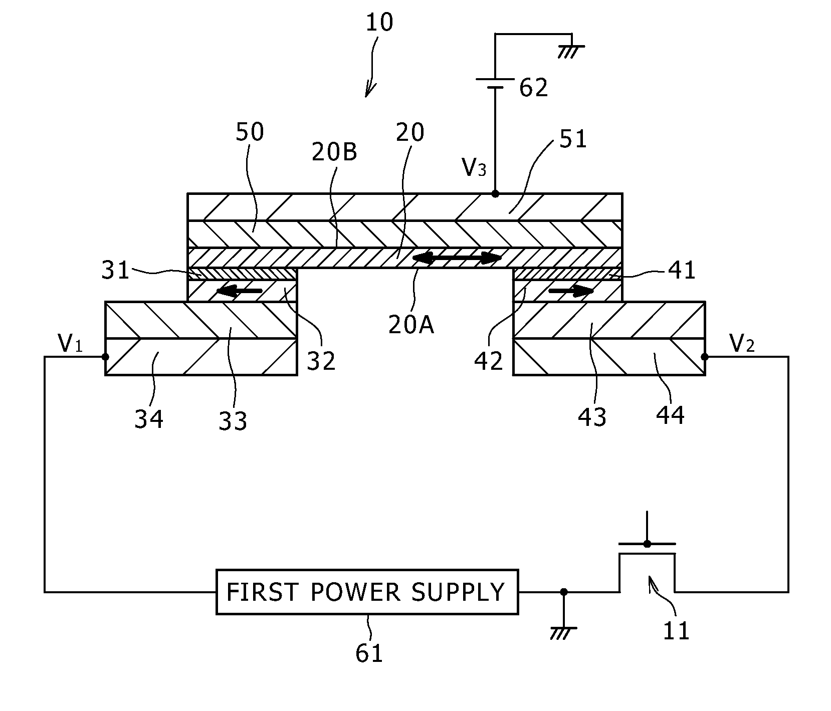
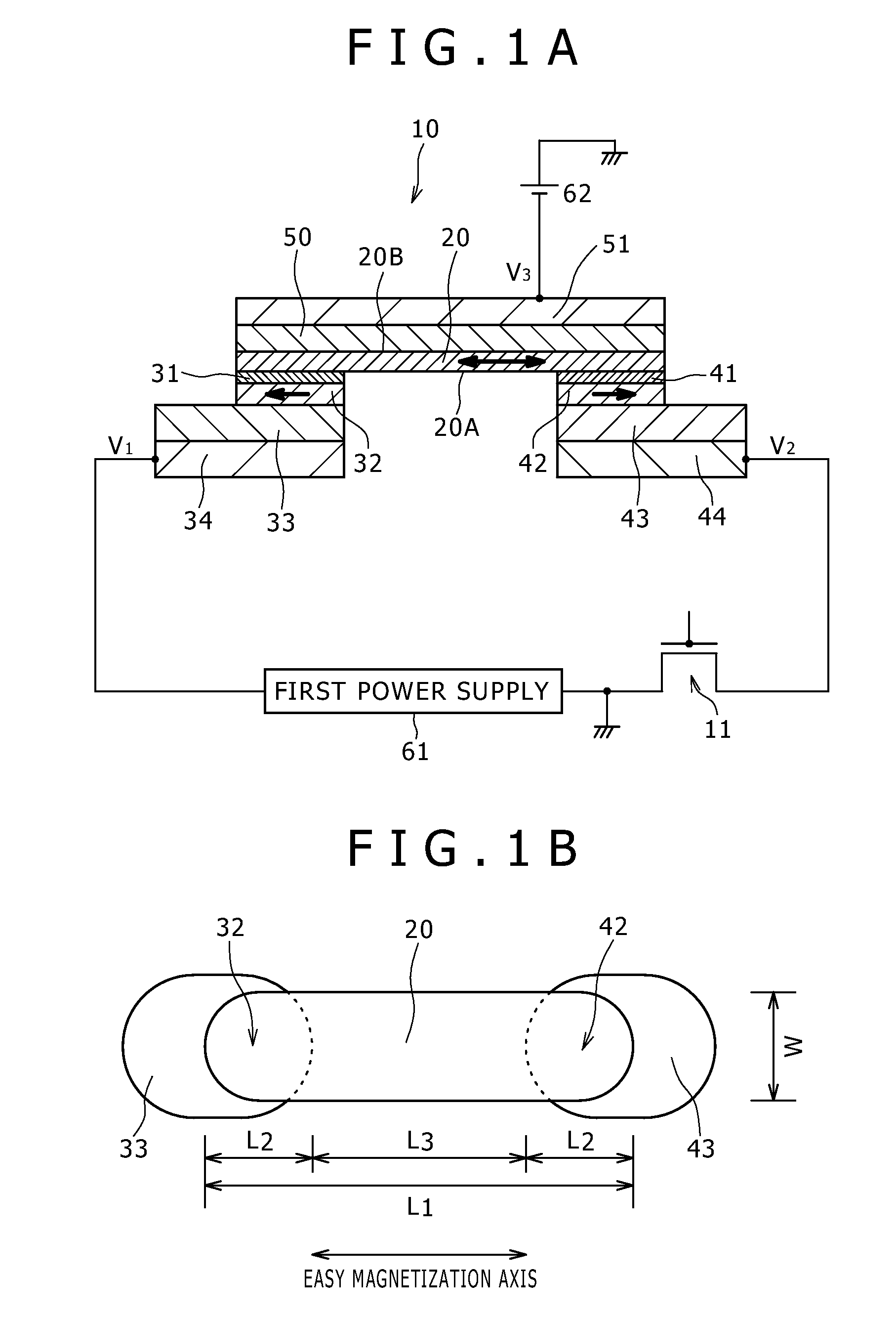
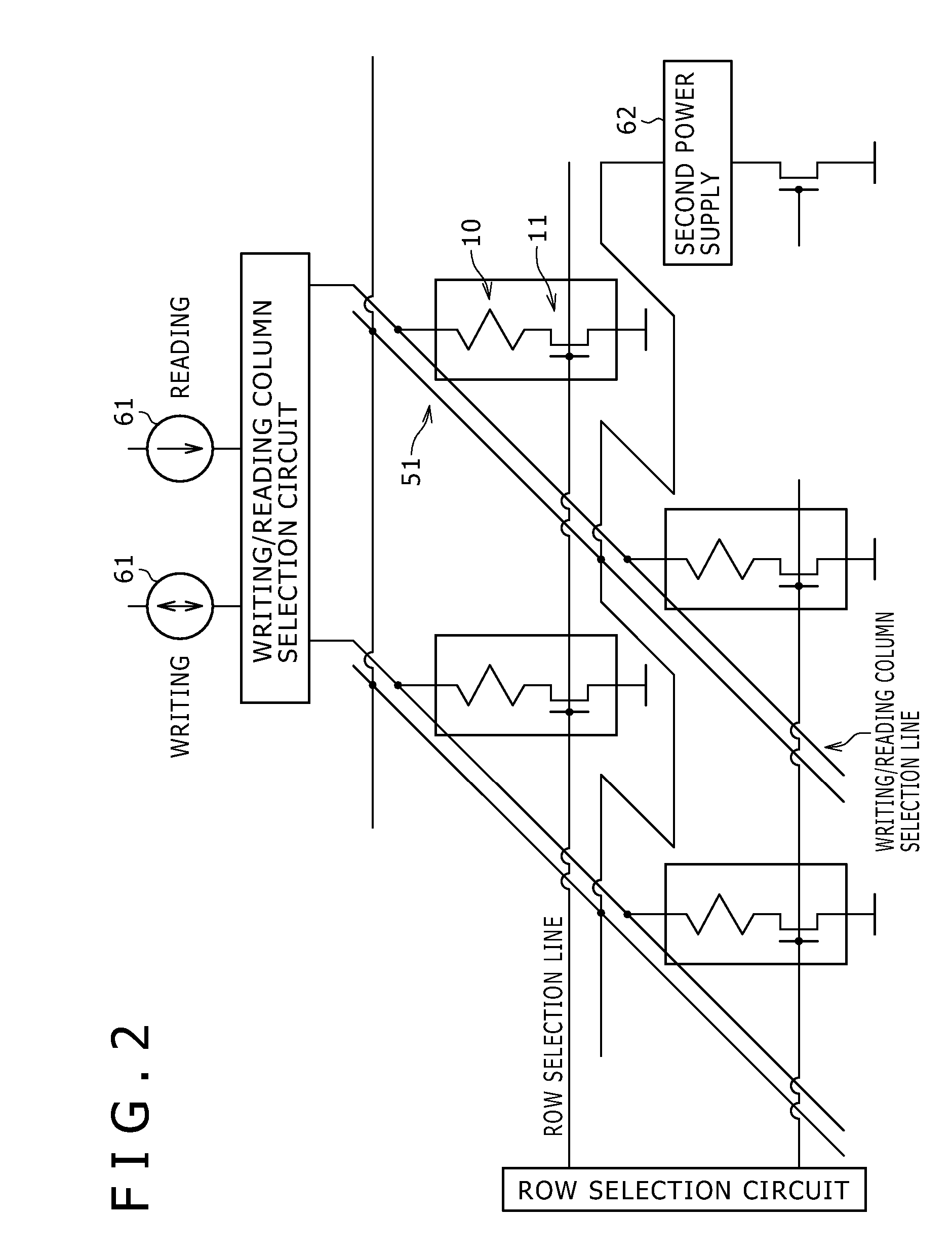
[0046]A first embodiment of the present invention relates to a spin-injection magnetoresistance effect element, and more specifically to a spin-injection magnetoresistance effect element applied to MRAM. A spin-injection magnetoresistance effect element 10 according to the first embodiment has a three-terminal spin transfer element structure that is referred to also as a voltage-assisted spin-injection magnetization reversal structure. FIG. 1A is a conceptual diagram illustrating the element 10. FIG. 1B is a schematic diagram illustrating the arrangement of a magnetization reversal layer, a first magnetization reference layer and a second magnetization reference layer in the element 10. FIG. 2 illustrates an equivalent circuit of the MRAM. FIG. 3 is a schematic sectional view illustrating part of the MRAM. Turning now to FIG. 1A, the spin-injection magnetoresistance effect element 10 includes (A) a magnetization reversal layer (referred to also as a free layer) 20 that has a first f...

second embodiment

[0073]The second embodiment is obtained by modifying part of the first embodiment. A spin-injection magnetoresistance effect element of the second embodiment is different from an element of the first embodiment in that in the second embodiment, a synthetic ferri-magnetic structure is employed for either one of the first and second magnetization reference layers. In the following description, a first magnetization reference layer 132 has a synthetic ferri-magnetic structure. FIG. 6A is a conceptual diagram illustrating part of a spin-injection magnetoresistance effect element of the second embodiment. FIG. 6B is an enlarged conceptual diagram illustrating the first magnetization reference layer 132 and other layers in the spin-injection magnetoresistance effect element of the second embodiment. It should be noted that a structure in which the second magnetization reference layer 42 has a synthetic ferri-magnetic structure is also available.

[0074]In the second embodiment, the first ma...

third embodiment

[0083]The third embodiment is also obtained by modifying part of the first embodiment. A spin-injection magnetoresistance effect element of the third embodiment is different from an element of the first embodiment in that in the third embodiment, first and second magnetization reference layers 32 and 42 have sufficiently high magnetic anisotropy energy (Ku·V), and therefore the first and second antiferromagnetic layers 33 and 43 are absent. FIG. 8A is a conceptual diagram illustrating a spin-injection magnetoresistance effect element according to the third embodiment.

[0084]The expression that the magnetic anisotropy energy (Ku·V) is “sufficiently high” means the following states:[0085](1) The magnetization directions of the first and second magnetization reference layers 32 and 42 overlapping with the magnetization reversal layer 20 can be parallel to the easy magnetization axis of the magnetization reversal layer 20. That is, the magnetization reference layers 32 and 42 maintain a ...


PUM

PropertyMeasurementUnit
sizeaaaaaaaaaa
currentaaaaaaaaaa
currentaaaaaaaaaa

Abstract

A spin-injection magnetoresistance effect element that can avoid use of a large writing current and allows use of a large reading current. The spin-injection magnetoresistance effect element includes layers that may exhibit a tunnel magnetoresistance effect and layers that may exhibit a giant magnetoresistance effect.

Description

CROSS REFERENCES TO RELATED APPLICATIONS[0001]The present invention contains subject matter related to Japanese Patent Application JP 2005-087950 filed in the Japanese Patent Office on Mar. 25, 2005, the entire contents of which being incorporated herein by reference.BACKGROUND OF THE INVENTION[0002]The present invention relates to a spin-injection magnetoresistance effect element.[0003]Magnetic random access memory (MRAM) has been known as a non-volatile magnetic memory element of high speed, high integration, and low power consumption (refer to U.S. Pat. No. 6,081,445, for example). The MRAM employing a tunnel magnetoresistance (TMR) effect includes tunnel magnetoresistive elements that are coupled to selection transistors formed of MOS-FETs. In addition, bit lines are provided above the tunnel magnetoresistive elements, and word lines extending perpendicularly to the bit lines are provided below the tunnel magnetoresistive elements. The tunnel magnetoresistive element has a multi...

Claims


Application Information

Patent Timeline
Patent Type & Authority Patents(United States)
IPC IPC(8): G06K9/00G11B5/127G11C11/00G11C11/14
CPCB82Y25/00G01R33/093G11C11/16H01L43/08H01L27/228H10B61/22H10N50/10
Inventor YAGAMI, KOJIRO
Owner SONY CORP
Why Eureka
Try Eureka