Light emitting device

a technology of light-emitting devices and light-emitting devices, which is applied in the direction of semiconductor devices, basic electric elements, electrical apparatus, etc., can solve the problems of poor reproducibility of forward voltage and current, unstable forward voltage, etc., and achieve stable and low forward voltage , the effect of enhancing the brightness of the light-emitting devi

Active Publication Date: 2006-02-07
EPISTAR CORP
View PDF20 Cites 7 Cited by
  • Summary
  • Abstract
  • Description
  • Claims
  • Application Information

AI Technical Summary

Benefits of technology

[0007]An objective of the present invention is to provide a light emitting device structure with a transparent conductive layer sitting on the semiconductor layers, so no agent layer between the transparent conductive layer and the semiconductor layers is required to get stable operating voltage and excellent light transmission. In this invention, the transparent conductive layer can be any kind of metal oxide material, like ITO, NiO, ZnO, RuO2 or IrO2, etc., while their work function is higher than 4.5 eV after treatment when they are used in InGaN material devices. The top layer of semiconductor part comprises a hybrid superlattice structure, wherein the hybrid superlattice structure comprises a first supperlattice structure composed of two to five pairs of wide bandgap material layers and narrow bandgap material layers, such as AlGaN Layer / GaN Layer, located on a cladding layer. Since the voltage is determined by the first contact width proposed in this invention, not by the interface dopant concentration, the reliable steady voltage is predicted. The brightness of the light emitting device can be enhanced since the first supperlattice structure can spread hole carriers.
[0008]Another objective of the present invention is to provide a light emitting device, and the hybrid superlattice structure of the contact layer comprises a second supperlattice structure composed of one to two pairs of wide bandgap material layer and narrow bandgap material layer, such as GaN Layer / InGaN Layer, located on the first supperlattice structure. In this invention, the thickness, not the doping concentration, of the second supperlattice structure can provide a tunneling contact for p type carriers or n type carriers, the forward voltage difference can be designed and kept constant, so as to keep the forward voltage stable.
[0012]Because the first superlattice structure can spread carriers, and the carriers can tunnel the second superlattice structure, the brightness of the light emitting device can be enhanced, and a stable and low forward voltage can be obtained.

Problems solved by technology

The major technical concerns is to seek low and stable operating forward voltage (Vf), since it is not easy to form ohmic contact between the indium tin oxide and p type GaN.
However, the agent layer between the indium tin oxide and the p type GaN contact layer will absorb output light intensity, and the forward voltage is unstable during operation because the high doping concentration inside the agent layer results in carrier diffusion between the agent layer and the contact layer.
However, the aforementioned inventions all suffer a problem of poor reproducibility of forward voltage and current because of the difference of surface roughness of epiwafer or the variation of hydrogen passivation effect.

Method used


Image

  • Light emitting device
  • Light emitting device

Examples


Embodiment Construction

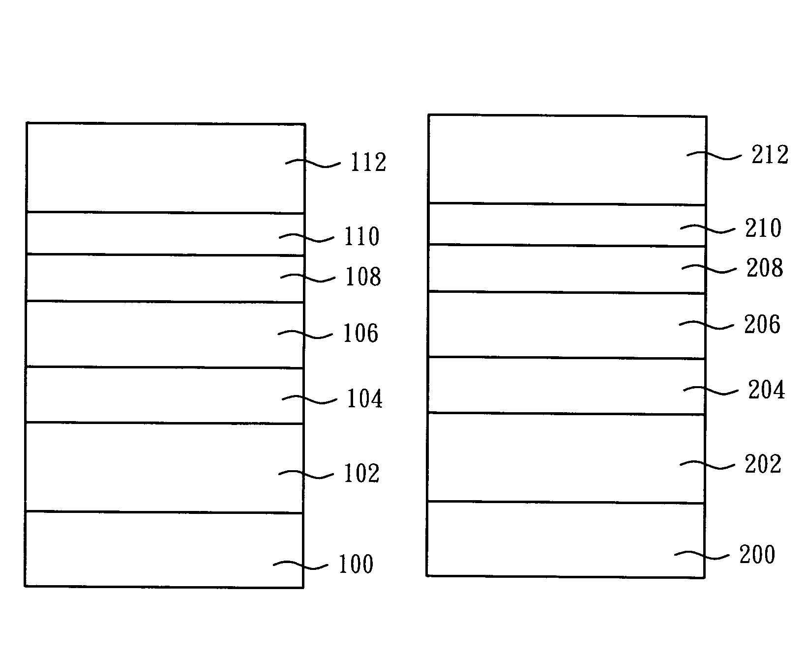
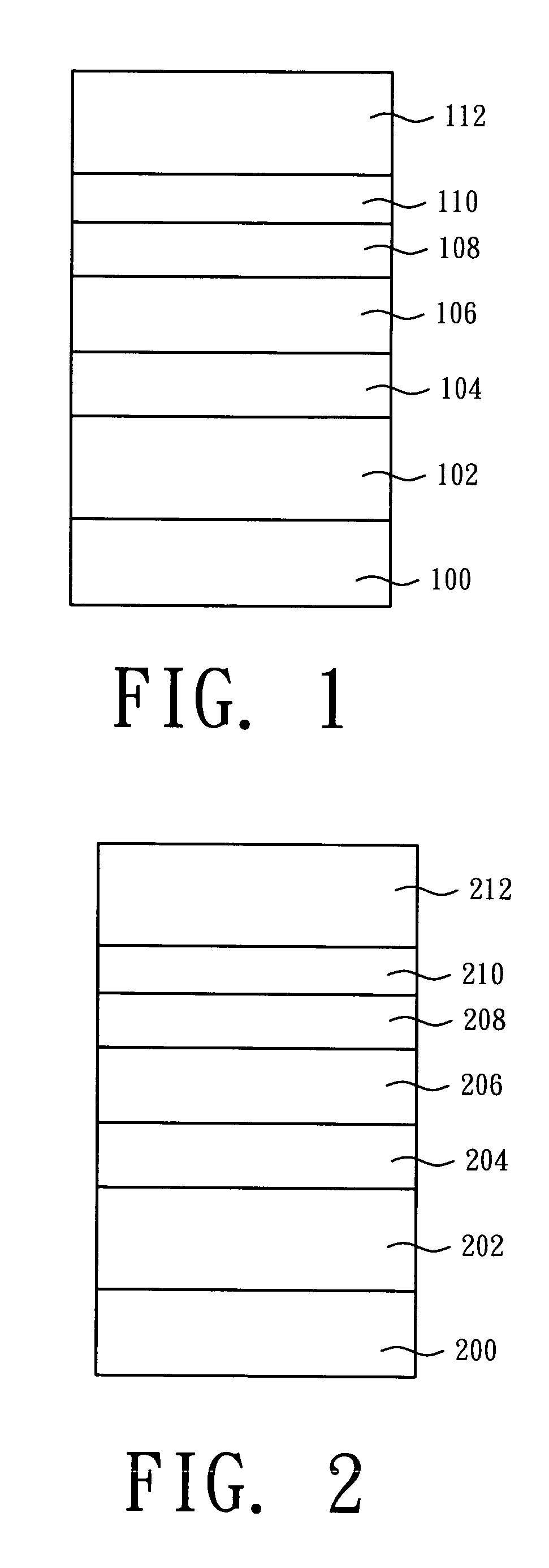
[0016]The present invention discloses a light emitting device comprising a contact layer composed of a hybrid superlattice structure which can spread hole carriers and provide tunneling contact for the carriers. In addition, an oxide transparent layer can be directly deposited on the contact layer. Therefore, the brightness of the light emitting device can be enhanced, and a stable and low forward voltage can be obtained. In order to make the illustration of the present invention more explicitly and completely, the following description is stated with reference to the accompanying drawings of FIG. 1 and FIG. 2.

[0017]Referring to FIG. 1, FIG. 1 illustrates a cross-sectional view of a light emitting device in accordance with a preferred embodiment of the present invention. The light emitting device structure of the present invention comprises a substrate 100 which is transparent, a n type semiconductor layer 102, an active layer 104, a p type cladding layer 106, a superlattice structu...


PUM


Abstract

A light emitting device is disclosed. The light emitting device comprises a contact layer and an oxide transparent layer located directly on the contact layer. The contact layer has a stacked structure formed by alternately stacking a plurality of nitride semiconductor layers having a wider bandgap and a plurality of nitride semiconductor layers having a narrower bandgap.

Description

FIELD OF THE INVENTION[0001]The present invention relates to a light emitting device, and more particularly, to a semiconductor light emitting device having high brightness and a low forward voltage.BACKGROUND OF THE INVENTION[0002]The metal oxide transparent conductive material, like indium tin oxide (ITO), nickel oxide (NiO) has been widely used on opto-electronic devices, such as thin film transistor liquid crystal display (TFT-LCD), organic light emitting device (OLED) and light emitting device especially in InGaN series material. It is used as a conductive window layer of the opto-electronic device for current spreading and light transmission. The major technical concerns is to seek low and stable operating forward voltage (Vf), since it is not easy to form ohmic contact between the indium tin oxide and p type GaN.[0003]The forward voltage is lowered by applying an agent layer between the indium tin oxide and p type GaN. For example, the U.S. Pat. No. 5,977,566 filed by Okazaki...

Claims


Application Information

Patent Timeline
Patent Type & Authority Patents(United States)
IPC IPC(8): H01L29/22H01L29/221H01L29/225H01L29/24H01L29/739H01L33/04H01L33/14H01L33/32
CPCH01L33/04H01L33/32H01L33/14
Inventor TU, CHUAN-CHENGYOUNG, CHENG-CHUNGHUANG, PAO-IWU, JEN-CHAU
Owner EPISTAR CORP
Why Eureka
Try Eureka