Wiring structure and manufacturing method therefor, semiconductor device including wiring structure and wiring board

a manufacturing method and wiring structure technology, applied in semiconductor devices, semiconductor/solid-state device details, electrical devices, etc., can solve the problems of complex manufacturing process, no transmission line structure used in semiconductor devices, and increase manufacturing costs, so as to simplify manufacturing processes

Inactive Publication Date: 2006-02-07
SANYO ELECTRIC CO LTD
View PDF10 Cites 3 Cited by
  • Summary
  • Abstract
  • Description
  • Claims
  • Application Information

AI Technical Summary

Benefits of technology

[0011]An object of the present invention is to provide a wiring structure including a transmission line structure capable of simplify...

Problems solved by technology

Therefore, no transmission line structure is employed in the chip of the semiconductor device.
Therefore, the manufacturing process is complicated and the manufacturing cost is increased.
Also when the structure shown in FIG. 13 or 14 is formed as the wire in the chip of the semiconductor device, the patterning step including lith...

Method used


Image

  • Wiring structure and manufacturing method therefor, semiconductor device including wiring structure and wiring board
  • Wiring structure and manufacturing method therefor, semiconductor device including wiring structure and wiring board
  • Wiring structure and manufacturing method therefor, semiconductor device including wiring structure and wiring board

Examples


first embodiment

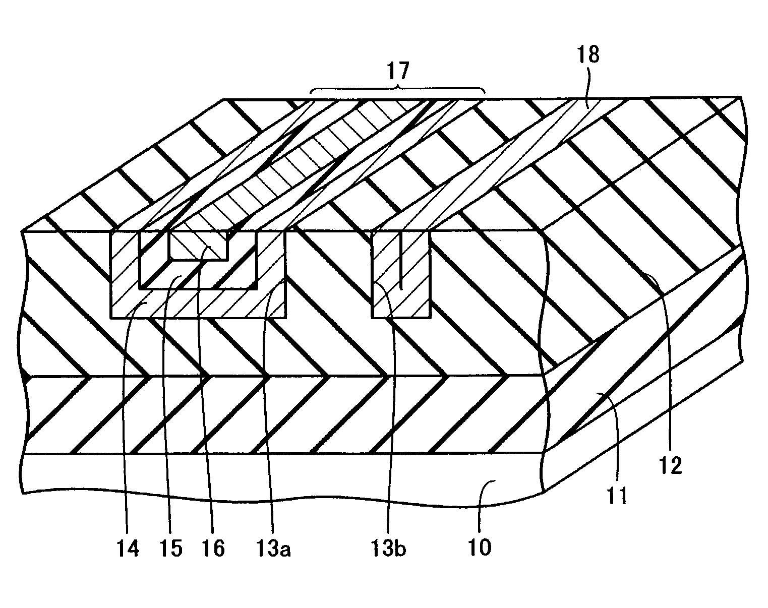
[0050](First Embodiment)

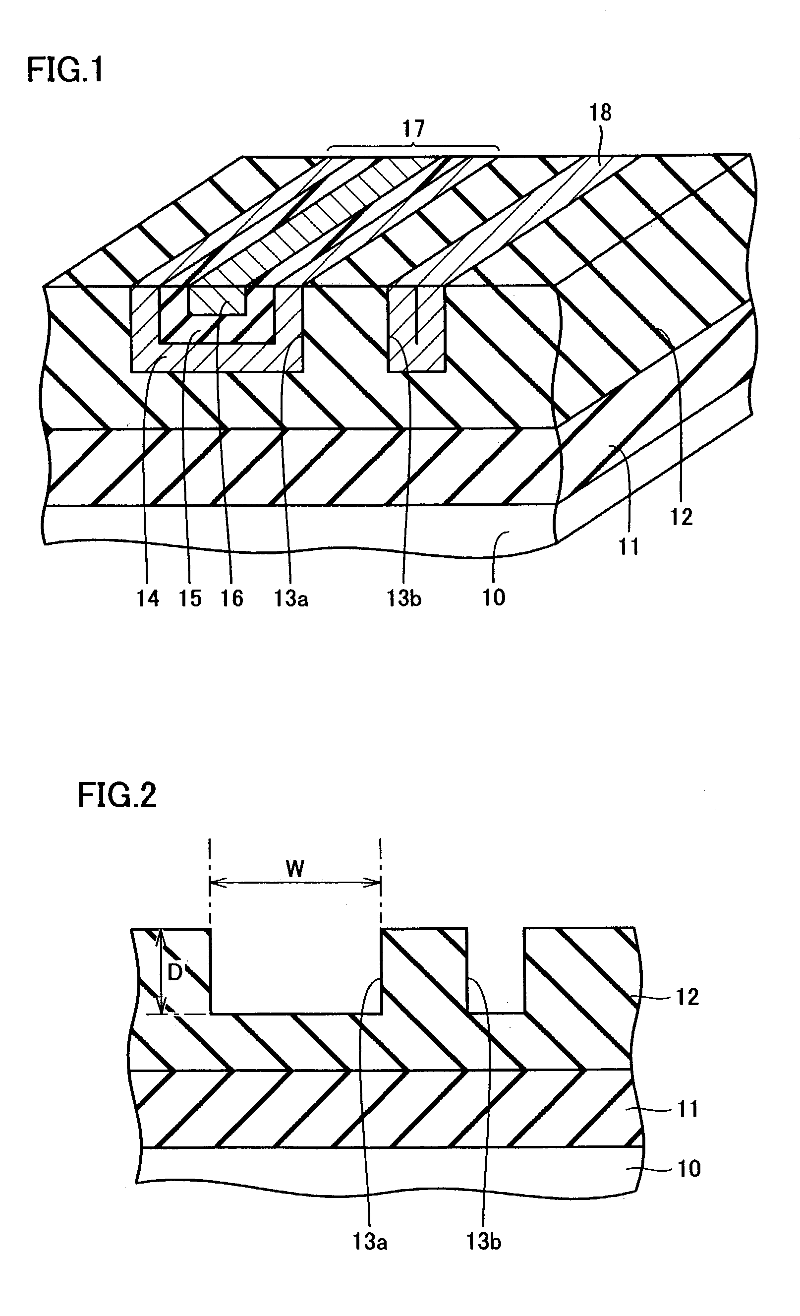
[0051]The structure of a semiconductor device including a wiring structure according to a first embodiment of the present invention is described with reference to FIG. 1. In the semiconductor device according to the first embodiment, an underlayer 11 consisting of an SiO2 film is formed on a semiconductor substrate 10, as shown in FIG. 1. An insulator film 12 having a thickness of about 2 μm to about 20 μm is formed on the underlayer 11. The insulator film 12 is an example of the “first insulator film” in the present invention.

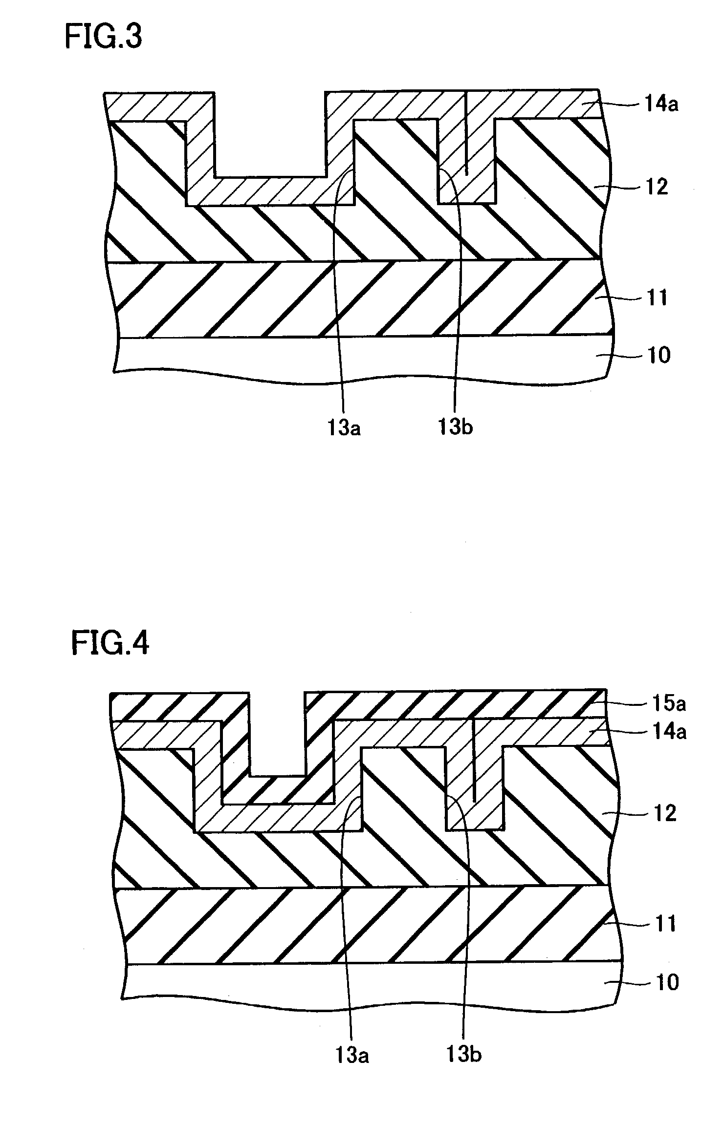
[0052]According to the first embodiment, rectangular trenches 13a and 13b are formed on the surface of the insulator film 12 at a prescribed interval. The trench 13a has a width of about 1 μm to about 10 μm and a depth of about 1 μm to about 10 μm. The trench13b is smaller in width than and identical in depth to the trench 13a. An outer wire 14 of copper, an insulator film 15 consisting of an SiO2 film and an inner wire 16 of copper are...

second embodiment

[0081](Second Embodiment)

[0082]A second embodiment of the present invention is now described with reference to FIG. 11. In the second embodiment, the present invention is applied to a wiring board 61 for mounting an integrated circuit device (semiconductor device), dissimilarly to the aforementioned first embodiment.

[0083]According to the second embodiment, an insulator film 62 is formed on the wiring board 61. Rectangular trenches 63a and 63b are formed on the surface of the insulator film 62. The trenches 63a and 63b are similar in dimension and shape to the trenches 13a and 13b of the semiconductor device according to the first embodiment shown in FIG. 1 respectively. An outer wire 64 is concavely formed along the inner surfaces of the rectangular trench 63a. An insulator film 65 is concavely formed along the inner surfaces of the outer wire 64. An inner wire 66 is formed to fill up the concave portion of the insulator film 65. The inner and outer wires 66 and 64 form a wire pair...


PUM

PropertyMeasurementUnit
Thicknessaaaaaaaaaa

Abstract

A wiring structure including a transmission line structure capable of simplifying a manufacturing process is obtained. This wiring structure comprises a first trench formed on a first insulator film provided on a substrate, a first wire formed in the extensional direction of the first trench along at least part of the inner surface of the first trench and a second wire formed to be opposed to the first wire through a second insulator film for forming a transmission line for transmitting signals with the first wire. The first wire, the second insulator film and the second wire are embedded in the first trench. This wiring structure is manufactured through a single lithography step, a single etching step and a single resist removing step for forming the first trench and a single CMP step, whereby the manufacturing process is simplified.

Description

BACKGROUND OF THE INVENTION[0001]1. Field of the Invention[0002]The present invention relates to a wiring structure and a manufacturing method therefor, a semiconductor device including the wiring structure and a wiring board, and more specifically, it relates to a wiring structure serving as a transmission line for transmitting signals and a manufacturing method therefor, a semiconductor device including the wiring structure and a wiring board.[0003]2. Description of the Background Art[0004]Following the recent shrinkage of design rule of semiconductor devices, the frequencies of signals have approached to the gigahertz (GHz) band, partially exceeding 1 GHz. When the frequency of a signal reaches the GHz band, it is difficult to handle a signal wire as a lumped constant circuit generally employed for designing a semiconductor device and hence the signal wire must be handled as a distributed constant circuit. The term “lumped constant circuit” indicates a circuit handling inductors,...

Claims


Application Information

Patent Timeline
IPC IPC(8): H01L23/48C25D7/12H01L21/3205H01L21/768H01L23/52H01L23/522
CPCH01L21/76838H01L21/76877H01L23/5222H01L2924/3011H01L2924/0002H01L2924/00
Inventor OKAYAMA, YOSHIO
Owner SANYO ELECTRIC CO LTD
Why Eureka
Try Eureka