Cross point resistive memory array

a resistive memory array and cross-point technology, applied in the field of information storage devices, can solve problems such as read and write sensitivity problems

Active Publication Date: 2006-02-21
SAMSUNG ELECTRONICS CO LTD
View PDF3 Cites 121 Cited by
  • Summary
  • Abstract
  • Description
  • Claims
  • Application Information

AI Technical Summary

Problems solved by technology

However, since the junctions are essentially resistors, problems arise in read and write sensitivity as a result of shunt currents passing through junctions other than the selected junction.
However the equivalent circuit of each memory cell includes a tunnel gate surface effect transistor having non-uniform gate oxide built on the pillar diode structure.

Method used


Image

  • Cross point resistive memory array
  • Cross point resistive memory array
  • Cross point resistive memory array

Examples


Embodiment Construction

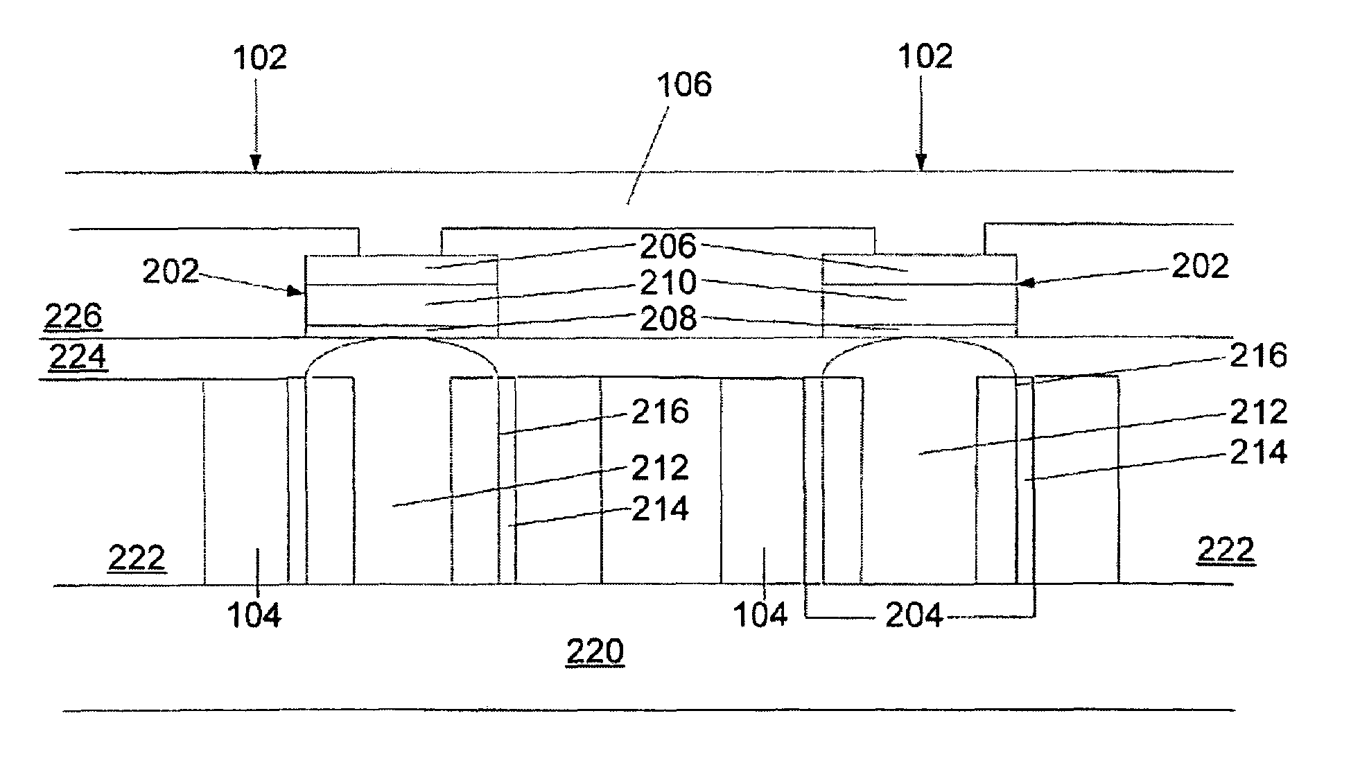
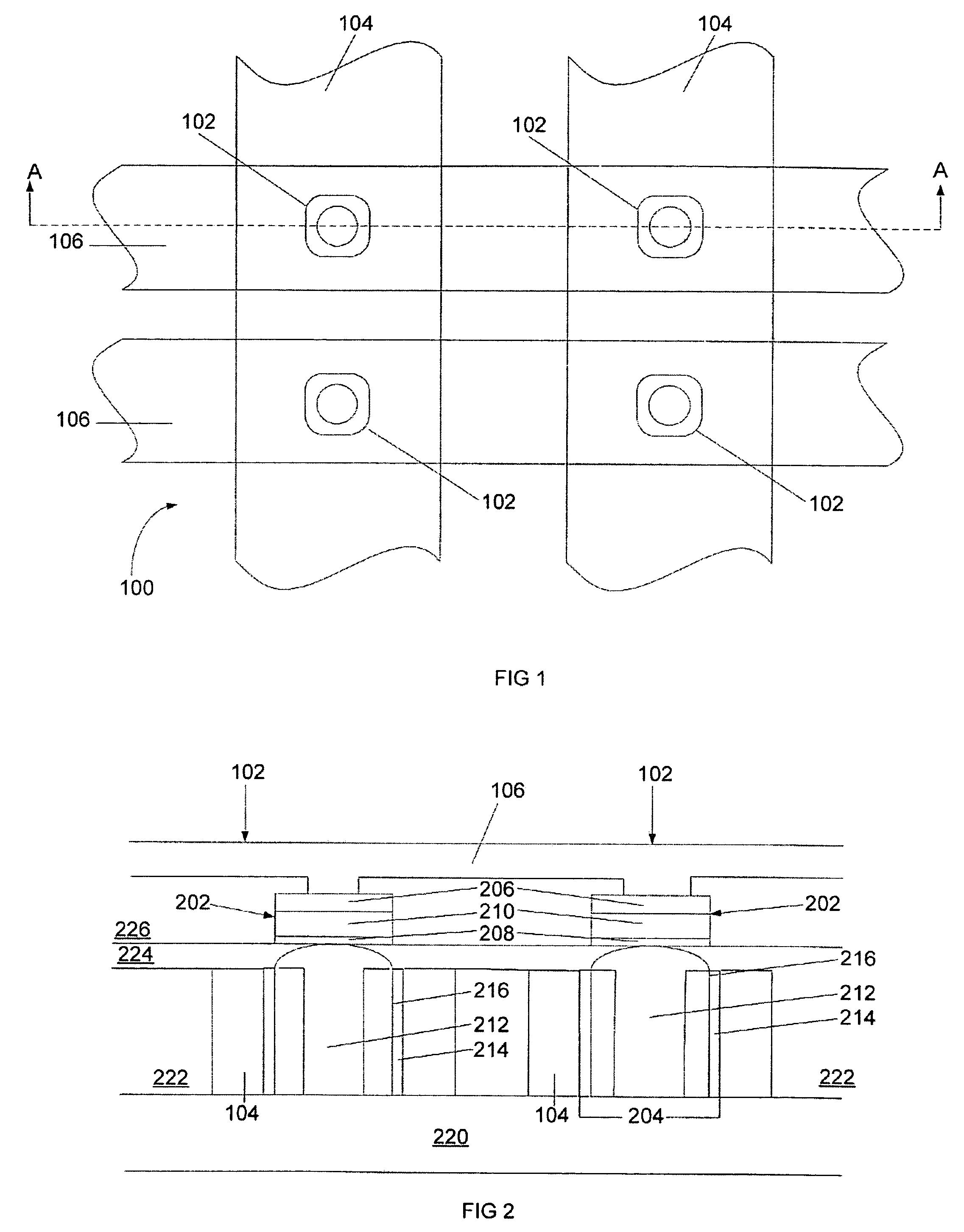
[0016]The figures illustrate an MRAM device but it will be appreciated that the device is not limited to MRAM and may include memory cells of the type including phase change memory cells, a resistive polymer memory cell, a polysilicon memory cell, or a write-once (eg. fuse based or anti-fuse based) resistive memory cell.

[0017]FIGS. 1 and 2 illustrate a preferred form of the magnetic random access memory device 100. As shown, the device includes four memory cells 102 arranged in a planar array. While only four memory cells have been shown in FIG. 1, it will be appreciated that the array may be many times larger.

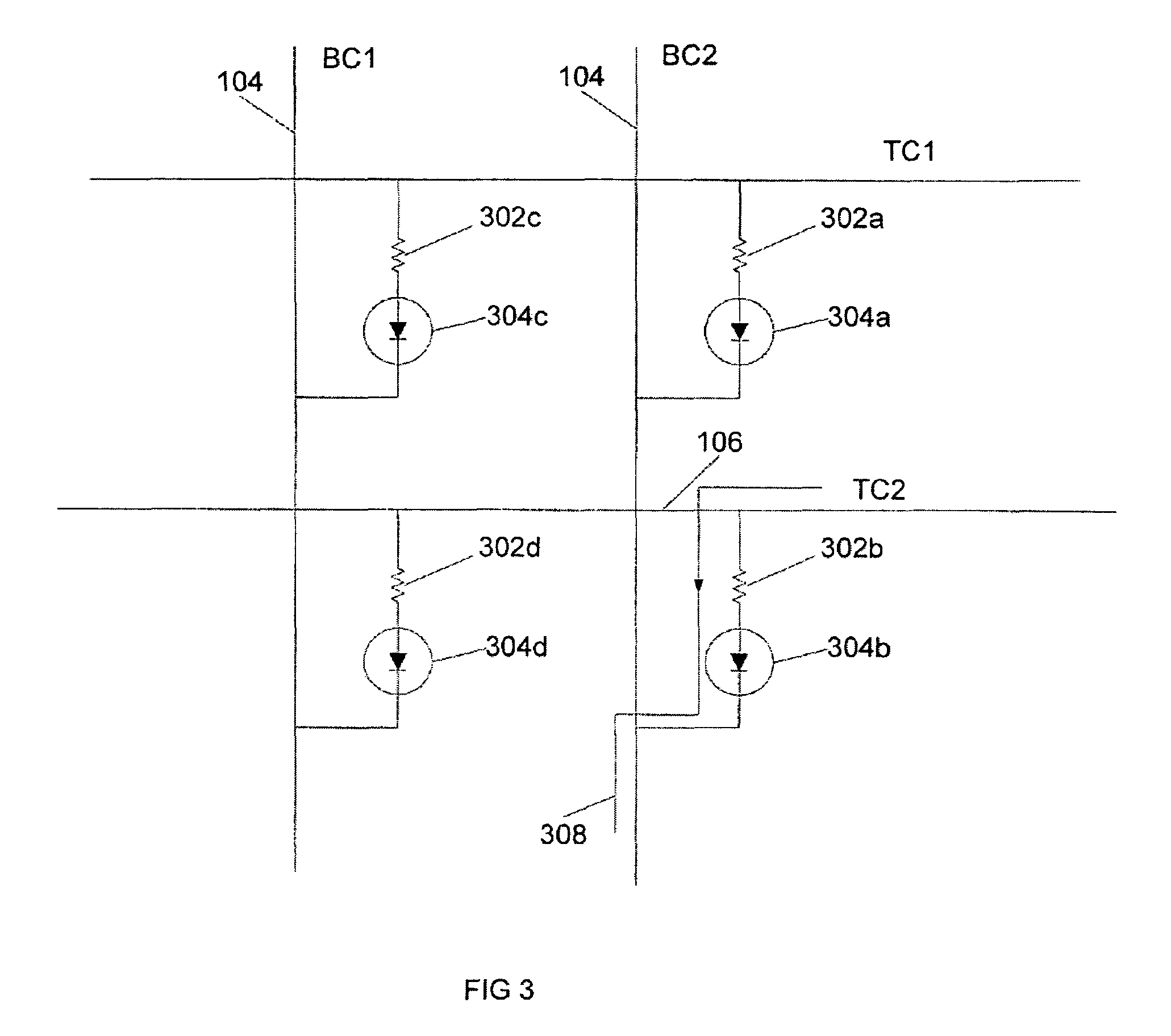
[0018]The memory cells 102 are cross-linked by bottom line conductors 104 and top line conductors 106. The line conductors are made from copper formed by a copper damascene process as will be explained further below.

[0019]As can be seen from FIG. 2, each of the memory cells 102 comprises a magnetic storage element 202 integrated with a current control element in a form of a di...


PUM


Abstract

A cross point resistive memory array has a first array of cells arranged generally in a plane. Each of the memory cells includes a memory storage element and is coupled to a diode. The diode junction extends transversely to the plane of the array of memory cells.

Description

RELATED APPLICATIONS[0001]This patent application is a continuation-in-part (CIP) of patent application Ser. No. 10 / 764,052, titled “CROSS POINT RESISTIVE MEMORY ARRAY”, filed Jan. 23, 2004, now abandoned.FIELD OF THE INVENTION[0002]The present invention relates information storage devices. More specifically, the invention relates to cross point resistive memory arrays. In particular, although not exclusively, the invention may have application to magnetic random access memory (“MRAM”) devices.BACKGROUND[0003]Many different resistive cross point memory cell arrays have been proposed, including resistive cross point memory cell arrays having MRAM elements, phase change memory elements, resistive polymer memory elements, polysilicon memory elements, and write-once (eg. fuse based or anti-fuse based) resistive memory elements.[0004]Consider the example of an MRAM device including a resistive cross point array of spin dependent tunnelling (SDT) junctions, word lines extending along rows...

Claims


Application Information

Patent Timeline
Patent Type & Authority Patents(United States)
IPC IPC(8): H01L29/76G11C7/02G11C11/16H01L27/22H01L27/24
CPCG11C11/16H01L27/224H01L27/24H10B61/10H10B63/00
Inventor PERNER, FREDERICK A.SHARMA, MANISH
Owner SAMSUNG ELECTRONICS CO LTD
Why Eureka
Try Eureka