Plasma display device and method of producing the same

a technology of plasma and display device, which is applied in the manufacture of electrode systems, electric discharge tubes/lamps, instruments, etc., can solve the problems of lowering luminance, fluctuation of discharge start voltage or luminance, and difficulty in reliability, so as to improve reliability and life, lowering luminance, and lowering luminance

Inactive Publication Date: 2006-02-21
SONY CORP
View PDF5 Cites 8 Cited by
  • Summary
  • Abstract
  • Description
  • Claims
  • Application Information

AI Technical Summary

Benefits of technology

[0009]The present inventors, as a result of their earnest studies for attaining the above object, have found out that when the trap density and / or the movable metallic ion density in the dielectric layer is set to be not more than a predetermined value; the fluctuation of discharge start voltage (driving voltage fluctuation) and the lowering of luminance would not easily be generated, and the reliability and life are enhanced. Based on the finding, the present invention has been completed. It is considered that the fluctuation of discharge start voltage (driving voltage fluctuation) and the lowering of luminance would not easily occur and the reliability and life are enhanced when the trap density and / or the movable metallic ion density in the dielectric layer is set to be not more than a predetermined value, because under this condition the sputtering of the protective film due to the potential generated by the electrons trapped in the traps can be obviated. Or, it is considered that the reason is that where the film quality of the dielectric layer is thus enhanced, the amount of the electric charges trapped in the dielectric layer is reduced, and the influence of the potential generated by the trapped electric charges can be reduced.
[0010]In addition, the present inventors have found out that when the trap density and / or the movable metallic ion density in the dielectric layer is set to be not more than a predetermined value, it is possible to prevent the fluctuation of voltage according to the position in the screen, which is considered to be a cause of the burning phenomenon of the screen.
[0015]Namely, it is possible to set the electric field strength to be comparatively low and to reduce largely the amount itself of electric charges injected into the dielectric layer by, for example, setting the thickness of the dielectric layer to be as large as about 20 to 40 μm. As a result, the generation of a negative potential due to the injected electric charges can be restrained, and acceleration of the sputtering of the protective layer can be prevented. In addition, fluctuation of the electric charge distribution can be restrained. Besides, by setting the electric field strength impressed on the dielectric layer to be low, fluctuation of the in-film distribution of the electric charges already injected into the dielectric layer can also be obviated. Therefore, it suffices to set the trap density in the dielectric layer to be not more than 1×10¹⁸ pieces / cm3 or to set the movable metallic ion density in the dielectric layer to be not more than 1×10¹⁸ pieces / cm3.
[0019]It is preferable that a barrier layer having a thickness of several nm to several tens of nm is provided between a bus electrode formed along the longitudinal direction of the discharge sustaining electrode and the dielectric layer, for preventing the diffusion of metal from the bus electrode into the dielectric layer or for preventing the injection of carriers. The provision of the barrier layer has the effect of preventing the diffusion of the metallic ions into the dielectric layer, thereby preventing the movable metallic ion density in the dielectric layer from increasing. For example, such metals as Ag, Na, Cr, Cu, Co, Fe, and Ni are liable to become movable ions. Therefore, in the case where the dielectric layer composed of a low melting point glass or the like is formed on the inside of the bus electrode consisting of a metallic electrode by a coating and firing method, it is preferable to provide the barrier layer, for preventing the diffusion of the metal from the bus electrode. As the barrier layer, for example, a film of silicon oxynitride (SiON), which is a nitrogen-containing silicon oxide, a film of titanium nitride (TiN) or the like is used.

Problems solved by technology

However, in the AC type plasma display device with the dielectric layer formed by the paste printing method, there is the problem of deterioration of the protective film.
Therefore, in the AC type plasma display device in which a thin dielectric layer composed of a low melting point glass is formed by the paste printing method, fluctuation of discharge start voltage or lowering of luminance would easily be generated due to the sputtering of the protective layer, resulting in difficulties on the basis of reliability.

Method used


Image

  • Plasma display device and method of producing the same
  • Plasma display device and method of producing the same
  • Plasma display device and method of producing the same

Examples


actual example 1

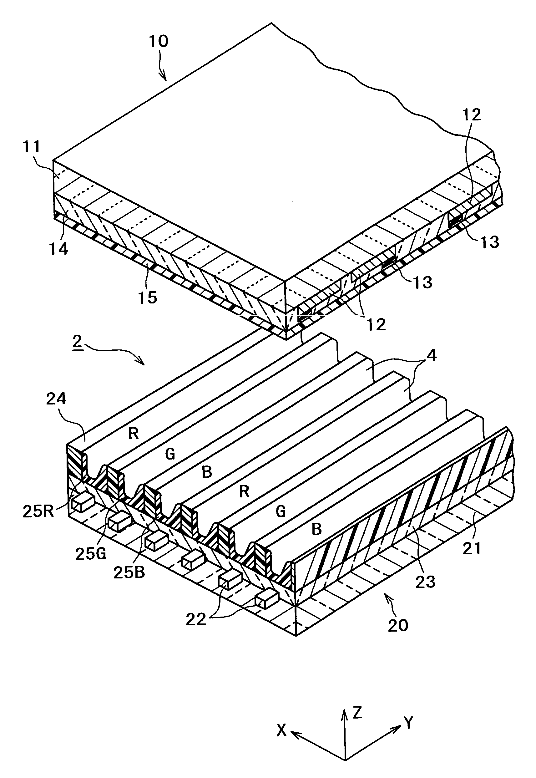
[0105]A first panel 10 was produced by the method as follows. First, an ITO layer was formed by a sputtering method, for example, on the entire surface of a first substrate 11 formed of a high strain point glass or a soda glass, and the ITO layer was patterned into a stripe form by photolithography technique and etching technique, whereby a plurality of pairs of discharge sustaining electrodes 12 were formed.

[0106]Next, an aluminum film was formed on the entire surface of the inside surface of the first substrate 11 by, for example, a vapor deposition method, and the aluminum film was patterned by photolithography technique and etching technique, to form bus electrodes 13 along an edge portion of each of the discharge sustaining electrodes 12.

[0107]Thereafter, a dielectric layer 14 composed of a silicon oxide (SiO2−x (0≦x11 provided with the bus electrodes 13. The dielectric layer 14 was formed by use of an RF sputtering method using an SiO2 target, in which the partial pressure (O2...

actual example 2

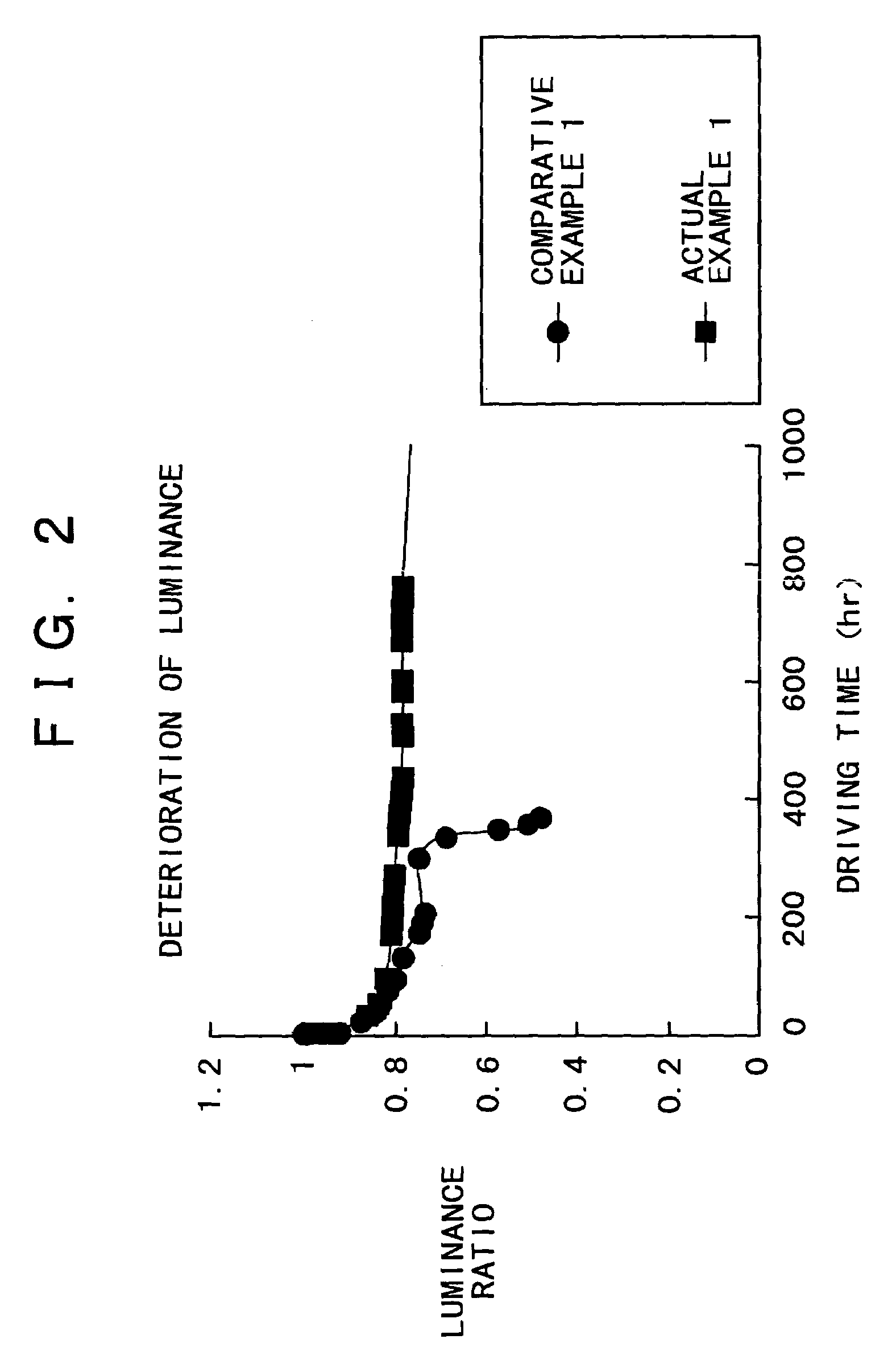
[0117]A plasma display device was assembled in the same manner as in Actual Example 1, except that the silicon oxide layer constituting the dielectric layer 14 was formed by a plasma CVD method using SiH4 and N2O as materials. When the same tests as in Actual Example 1 were conducted, the results similar to those in Actual Example 1 were obtained. The trap density in the dielectric layer in this example was 1×10¹⁶ pieces / cm3.

actual example 3

[0118]A plasma display device was produced in the same manner as in Actual Example 1, except that the dielectric layer 14 was formed by CVD using SiH4 and NH3+N2O so that the film constitution of the dielectric layer 14 would be SiON. The same measurements as in Actual Example 1 were conducted, except that the driving voltage was 210 V.

[0119]The trap density in the dielectric layer 14 was 1×10¹⁷ pieces / cm3. The results of luminance deterioration test and voltage life characteristic test were similar to those in Actual Example 1.


PUM


Abstract

A plasma display device such that fluctuation of discharge start voltage and lowering of luminance would not easily occur, the burning phenomenon of the screen is suppressed, and excellent reliability and long life can be secured, and a method of producing the same, are disclosed. The plasma display device comprises a first panel (10) provided with discharge sustaining electrodes (12) and a dielectric layer (14) on the inside thereof, and a second panel (20) laminated on the first panel (10) so that discharge spaces (4) are formed on the inside of the first panel (10), and the trap density and / or the movable metallic ion density in the dielectric layer (14) is not more than 1×10¹⁸ pieces / cm3, preferably not more than 1×10¹⁷ pieces / cm3.

Description

TECHNICAL FIELD[0001]The present invention relates to a plasma display device and a method of producing the same. More particularly, the present invention relates to a plasma display device having characteristic features as to the trap density and / or the movable metallic ion density of a dielectric film formed on sustaining electrodes or as to the trap density and / or the movable metallic ion density of a dielectric film formed on address electrodes, and a method of producing the same.BACKGROUND ART[0002]As a picture display device to be used in place of the cathode ray tube (CRT) which constitutes the main stream at present, a variety of flat panel type display devices have been investigated. Examples of such a flat panel type display device include liquid crystal display devices (LCD), electroluminescence display devices (ELD), and plasma display devices (PDP: plasma display panels). Among others, the plasma display devices have such merits as comparative easiness of an increase in...

Claims


Application Information

Patent Timeline
Patent Type & Authority Patents(United States)
IPC IPC(8): H01J17/49H01J9/02H01J11/12H01J11/22H01J11/24H01J11/26H01J11/34H01J11/38
CPCH01J9/02H01J11/38H01J11/12
Inventor KOJIMA, SHIGERUSUZUKI, TOSHIHARUSHIRAI, KATSUYA
Owner SONY CORP
Why Eureka
Try Eureka