Clocked D/A converter

a converter and clock technology, applied in pulse generators, pulse techniques, instruments, etc., can solve the problems of thermal hysteresis, thermal hysteresis is, therefore, unacceptable, and requires double power dissipation, and achieve the effect of overcoming the thermal hysteresis drawback of transistors q1 and q2

Inactive Publication Date: 2006-02-21
HRL LAB
View PDF22 Cites 7 Cited by
  • Summary
  • Abstract
  • Description
  • Claims
  • Application Information

AI Technical Summary

Benefits of technology

[0012]The present invention overcomes the prior art problems, enabling the thermal hysteresis drawback of transistors Q1 and Q2 to be overcome.

Problems solved by technology

DACs typically comprise many transistors, which can be subject to intersymbol interference coming, for example, from thermal hysteresis.
This behavior is called thermal hysteresis and could bring to intersymbol interference.
Thermal hysteresis is, therefore, unacceptable, because it could be the cause of possible distortion.
However, this configuration relies upon two separate current sources having two different phases, thus requiring double the power dissipation.
An additional problem is due to the different behavior of the two current sources, which causes a slightly different amount of current to go to the output from one clock phase to the next.

Method used


Image

  • Clocked D/A converter
  • Clocked D/A converter
  • Clocked D/A converter

Examples


Embodiment Construction

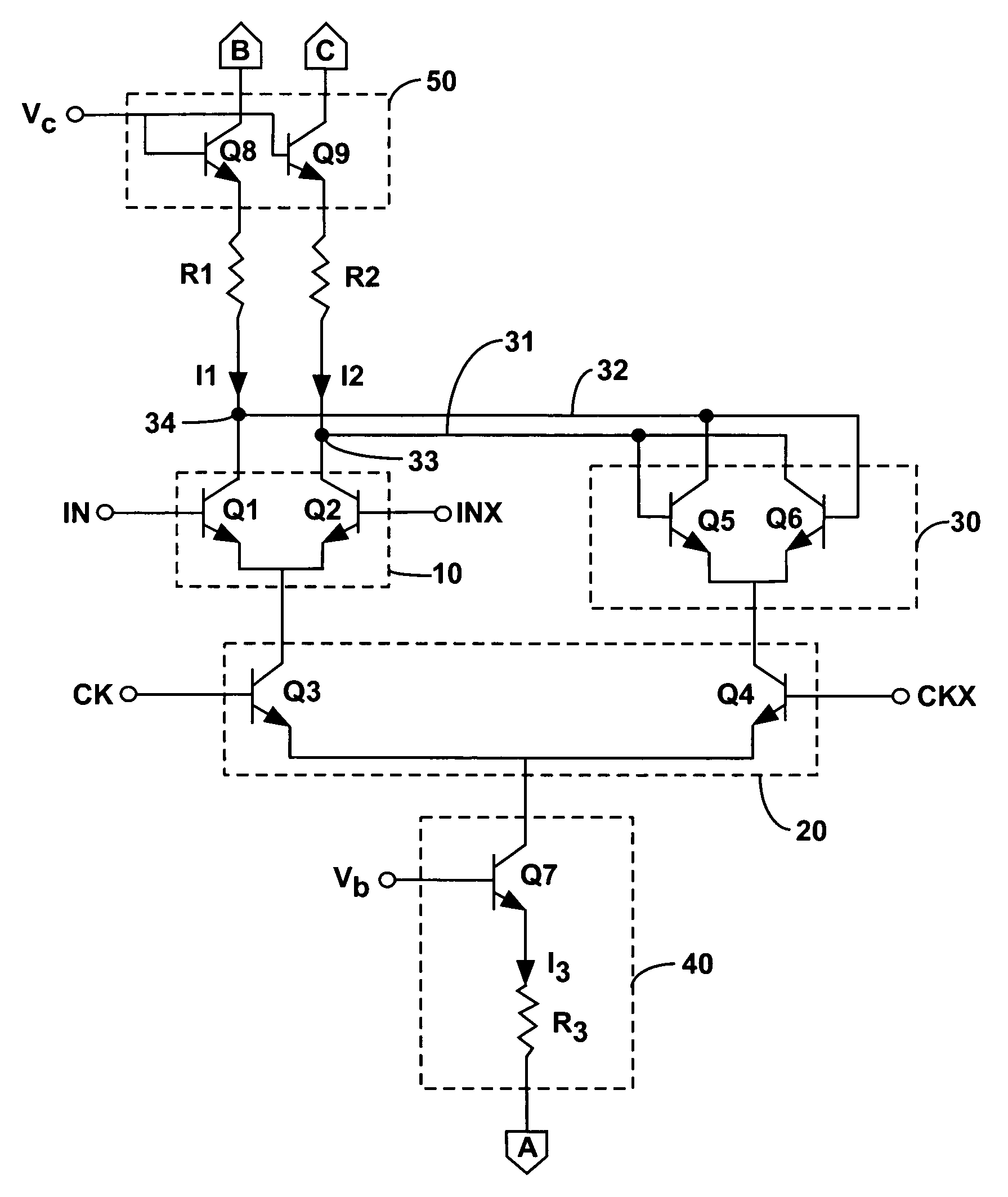
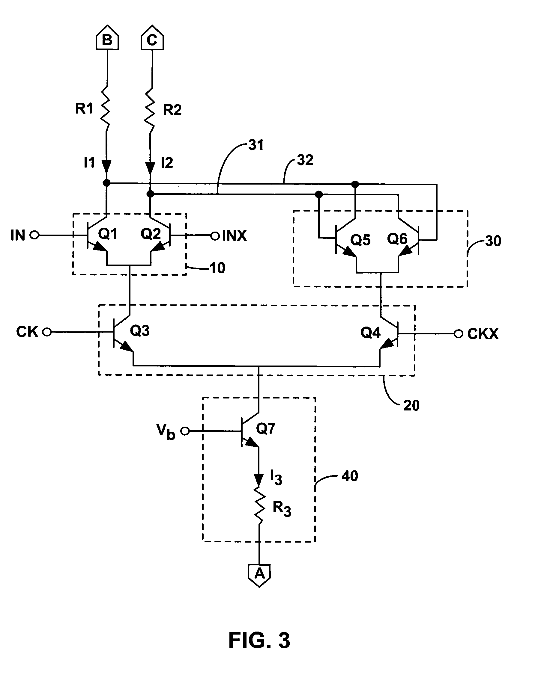
[0023]FIG. 3 shows a clocked NRTZ DAC according to a preferred embodiment of the present invention. A differential transistor pair 10 is connected with a clock circuit 20 and a bistable circuit 30. The bistable circuit 30 enables latching and operates as a positive feedback amplifier. The clock circuit 20 is also connected with a current generator 40 and the bistable circuit 30. The differential transistor pair 10 and the current generator 40 can be identical to those of the prior art shown in FIG. 1 of the present application. For example, FIG. 3 shows that the transistor pair 10 comprises npn bipolar transistors Q1 and Q2. The bases of Q1 and Q2 receive digital voltage input signals IN and INX, respectively. The emitters of Q1 and Q2 are connected together, and the analog current output of the DAC (currents I1, I2) is taken on the collectors of Q1 and Q2. The current source 40 comprises npn bipolar transistor Q7 and resistor R3, connected with the emitter of transistor Q7. The val...


PUM


Abstract

A digital-to-analog converter is disclosed, comprising an input / output circuit, a bistable circuit connected with the input / output circuit, a clock circuit connected with the input / output circuit and the bistable circuit, and a current generator circuit connected with the clock circuit. The clock circuit acts as a switch, providing current from the current generator either to the input / output circuit or to the bistable circuit. The digital input signal switches when the current generator provides current to the bistable circuit, and switching of the input signal is asserted at the output of the converter when the current generator provides current to the input / output circuit. Therefore, switching of a clock circuit signal, rather than switching of the digital input signal determines switching of the output signal, in order to reduce intersymbol interference of the converter associated with thermal hysteresis of some of the components of the converter.

Description

CROSS-REFERENCE TO RELATED APPLICATIONS[0001]Reference is made to the copending U.S. patent application Ser. No. 10 / 761,790 entitled “Clocked DAC Current Switch” by Albert E. Cosand, assigned to Raytheon Company, filed on the same date of the present application, the disclosure of which is incorporated herein by reference in its entirety.BACKGROUND[0002]1. Field[0003]The present invention relates to a digital-to-analog converter (DAC). More specifically, the present invention relates to a clocked DAC, where a clock prevents the DAC from emitting an output until the DAC inputs have fully switched.[0004]2. Related Prior Art[0005]DACs typically come in two forms, return to zero (RTZ) DACs, where signals return to zero also in absence of a data transition, and non return to zero (NRTZ) DACs, where signals do not return to zero, except during a data transition. DACs typically comprise many transistors, which can be subject to intersymbol interference coming, for example, from thermal hys...

Claims


Application Information

Patent Timeline
Patent Type & Authority Patents(United States)
IPC IPC(8): H03M1/66H03M1/06H03K3/2885H03K17/041H03M1/00H03M1/08H03M1/74
CPCH03K3/2885H03M1/0872H03M1/742H03K17/04106
Inventor KAPLAN, TODD
Owner HRL LAB
Why Eureka
Try Eureka