Simple step-up apparatus including level shift circuits capable of low breakdown voltage

a step-up apparatus and level shift circuit technology, applied in the direction of electric variable regulation, process and machine control, instruments, etc., can solve the problems of high cost and degrade integration of the step-up apparatus, and achieve the effect of low breakdown voltag

Active Publication Date: 2006-02-28
NEC LCD TECH CORP
View PDF5 Cites 37 Cited by
  • Summary
  • Abstract
  • Description
  • Claims
  • Application Information

AI Technical Summary

Benefits of technology

[0009]It is an object of the present invention to provide a step-up apparatus including level shift circuits capable of a low breakdown voltage.

Problems solved by technology

In the above-described first prior art step-up apparatus, however, since the (−K)-multiple charge pump circuit is complex, the step-up apparatus is high in cost.
However, since the transistors within the level shift circuit need to have a much higher breakdown voltage than that of the level shift circuits of the above-described first prior art step-up apparatus, the thickness of gate insulating layers of the transistors, the gate length and / or gate width of the transistors need to be large, which would degrade the integration.

Method used


Image

  • Simple step-up apparatus including level shift circuits capable of low breakdown voltage
  • Simple step-up apparatus including level shift circuits capable of low breakdown voltage
  • Simple step-up apparatus including level shift circuits capable of low breakdown voltage

Examples


first embodiment

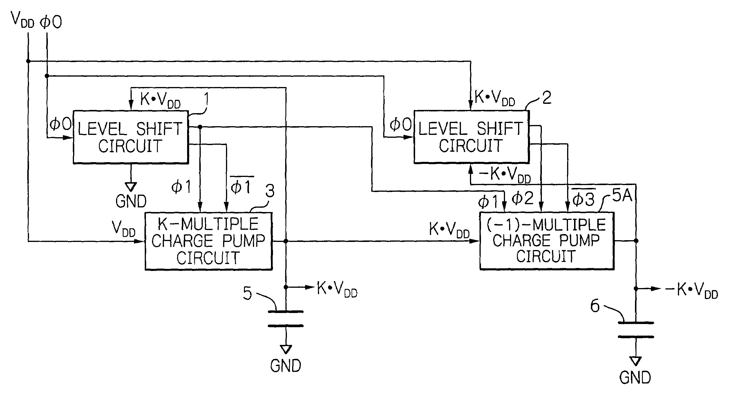
[0068]In FIG. 11, which illustrates the step-up apparatus according to the present invention, the (−K)-multiple charge pump circuit 4 of FIG. 1 is replaced by a (−1)-multiple charge pump circuit (or a polarity inverting circuit) 7A which receives the positive voltage K·VDD from the K-multiple charge pump circuit 3 to generate a negative voltage −K·VDD using the clock signals φ1, φ2 and {overscore (φ2)}.

[0069]The (−1)-multiple charge pump circuit 7A is illustrated in detail in FIGS. 12A and 12B which correspond to FIG. 10.

[0070]In FIG. 12A, the gates of the transistors 702 and 704 receive the clock signal φ1. On the other hand, the gate of the transistor 705 receives the clock signal φ2 while the gate of the transistor 703 receives the clock signal {overscore (φ2)}. That is, as shown in FIG. 13, the transistor 702 can be switched between a gate voltage of K·VDD−|Vtp| and a gate voltage of K·VDD, and the transistor 704 can be switched between a gate voltage of 0V and a gate voltage of...

second embodiment

[0074]In FIG. 14, which illustrates the step-up apparatus according to the present invention, the level shift circuit 2 of FIG. 11 is replaced by a level shift circuit 2B, and the (−1)-multiple charge pump circuit 7A of FIG. 11 is replaced by a (−1)-multiple charge pump circuit 7B.

[0075]The level shift circuit 2B is powered by the negative voltage −K·VDD and the ground voltage GND to level-shift the clock signal φ1 as shown in FIG. 15A and, thus generates a clock signal φ4 as shown in FIG. 15D.

[0076]The (−1)-multiple charge circuit 7B steps up the positive voltage K·VDD using the clock signals φ1 and φ4 as shown in FIGS. 15B and 15D to generate the negative voltage −K·VDD.

[0077]In FIG. 16, which is a detailed circuit diagram of the level shift circuit 2B of FIG. 14, a capacitor 208 and a diode 209 which also form a (−1)-multiple charge pump circuit or a polarity inverting circuit are added to the elements of the level shift circuit 2 of FIG. 4, and the CMOS inverter 207 of FIG. 4 is...

third embodiment

[0095]In FIG. 28, which illustrates the step-up apparatus according to the present invention, the clock signals φ2 and {overscore (φ2)} generated from the level shift circuit 2 of FIG. 11 are also supplied to the K-multiple charge pump circuit 3. In more detail, as illustrated in FIG. 29, which is a detailed circuit diagram of the K-multiple charge up circuit 3 of FIG. 28, the clock signal φ2 is supplied to the gate of the P-channel MOS transistor 311 and the clock signal {overscore (φ2)} is supplied to the P-channel MOS transistor 323.

[0096]As shown in FIG. 30, all the transistors 311, 322, 323 and 324 can be switched between a gate voltage of 0V and a gate voltage of K·VDD. Additionally, the transistors 311 and 323 can be switched between a gate voltage of −K·VDD and a gate voltage of VDD. In FIG. 28, use is made of this fact, so that the gate-to-source voltage can be increased to decrease the ON-resistance of the transistors 311 and 323 when they are turned ON.

[0097]An example of...


PUM


Abstract

In a step-up apparatus, a first level shift circuit receives a first clock signal to generate two phase-opposite second clock signals, and a second level shift circuit receives the first clock signal to generate two phase-opposite third clock signals. A charge pump circuit steps up a power supply voltage at a power supply voltage terminal using the second clock signals to generate a positive voltage, and a polarity inverting circuit inverts the positive voltage using the third clock signals to generate a negative voltage whose absolute value is the same as the positive voltage. A high level of the second clock signals is not higher than the positive voltage, and a low level of the second clock signals is not lower than a voltage at a ground terminal. A high level of the third clock signals is not higher than the power supply voltage, and a low level of the third clock signals is not lower than the negative voltage.

Description

BACKGROUND OF THE INVENTION[0001]1. Field of the Invention[0002]The present invention relates to a step-up apparatus or a DC-DC converter.[0003]2. Description of the Related Art[0004]Generally, a step-up apparatus is constructed by a charge pump circuit. On the other hand, in a liquid crystal display (LCD) apparatus, a positive voltage and a negative voltage are required to maintain the quality of the liquid crystal.[0005]A first prior art step-up apparatus for generating a positive voltage and a negative voltage is constructed by a first level shift circuit for receiving a first clock signal to generate two second clock signals opposite in phase with each other, a K (K=2, 3, . . . )-multiple charge pump circuit for generating the positive voltage of K·VDD using the second clock signals where VDD is a power supply voltage, a second level shift circuit for receiving the first clock signal to generate two third clock signals opposite in phase with each other, and a (−K)-multiple charg...

Claims


Application Information

Patent Timeline
Patent Type & Authority Patents(United States)
IPC IPC(8): G05F1/10G05F3/02H01L27/04H01L21/822H02M3/07
CPCH02M3/073H02M2003/076H02M2003/071H02M2001/009H02M1/009H02M3/071H02M3/076
Inventor NONAKA, YOSHIHIRO
Owner NEC LCD TECH CORP
Why Eureka
Try Eureka