Test circuit capable of testing embedded memory with reliability

a test circuit and memory technology, applied in the direction of instruments, coding, code conversion, etc., can solve the problems of the like of memory b>904/b>, the inability to correctly measure the set up and hold time, and the inability to correctly measure the access time of data reading when logic b>902/b> accesses memory b>904/b>

Inactive Publication Date: 2006-02-28
RENESAS TECH CORP
View PDF10 Cites 46 Cited by
  • Summary
  • Abstract
  • Description
  • Claims
  • Application Information

AI Technical Summary

Benefits of technology

[0016]It is an object of the present invention to provide a semiconductor integrated circuit device capable of correctly measuring timing conditions such as setup and hold times and an access time of an embedded memory using an external test apparatus.
[0017]It is another object of the present invention to provide a logic merged memory capable of correctly measuring timing conditions of a signal associated with access to the memory using a test apparatus.
[0018]It is still another object of the present invention to provide a semiconductor integrated circuit device with an embedded memory capable of correctly measuring setup and hold times and an access time of a desired signal / data of the embedded memory with high precision without increasing a test circuit scale.
[0023]Moreover, by taking in an output signal from the memory into a register circuit, a time point when data is outputted from the memory can be detected. Therefore, an access time can be measured with ease (an access time can be measured by measuring a time period required for the taking-in after application of a data output command).

Problems solved by technology

However, since access to memory 904 is made through signal switch circuit 910 and selection circuit 912, a problem arises that for example, set-up and hold times, an access time and the like of memory 904 cannot be correctly measured.
That is, the set up and hold times cannot be correctly measured due to an interconnection delay and a skew along this internal transfer path.
Furthermore, since data read out from memory 904 is detected externally by an external test apparatus through signal switch circuit 910, such a problem arises that an access time in data reading when logic 902 accesses memory 904 cannot be correctly measured.
This problem associated with the set up and hold times occurs not only on data but also on an address signal and a control signal instructing an operation mode in a similar manner.
Memory 904 is generally a synchronous memory operating in synchronization with a clock signal and if the set up and hold times can not be guaranteed, there arises a possibility of failing to correctly take in a command and write data.
Moreover, with respect to an access time either, there is a possibility that a high speed operation of logic 902 cannot be insured if correct measurement on an access time cannot be performed in data transfer from memory 904 to logic 902 in a case where data is transferred in synchronization with a high speed clock signal.

Method used


Image

  • Test circuit capable of testing embedded memory with reliability
  • Test circuit capable of testing embedded memory with reliability
  • Test circuit capable of testing embedded memory with reliability

Examples


first embodiment

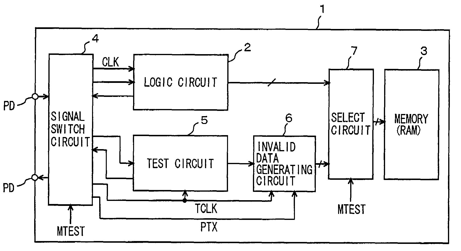
[0063]FIG. 1 is a diagram schematically showing an overall configuration of a semiconductor integrated circuit device according to a first embodiment of the present invention. In FIG. 1, a semiconductor integrated circuit device 1 includes: a logic circuit 2 performing a prescribed processing; a memory (RAM) 3 storing data required by logic circuit 2; a test circuit 5 communicating a test signal and data with a test apparatus outside semiconductor integrated circuit device 1 in a test mode; an invalid data generating circuit 6 selectively setting a test signal from test circuit 5 to an invalid state according to an asynchronous control signal PTX; a signal switch circuit 4 selectively coupling logic circuit 2 and test circuit 5 to external pads according to a test mode instructing signal MTEST; and a select circuit 7 selectively coupling output signals of logic circuit 2 and invalid data generating circuit 6 to memory 3 according to test mode instructing signal MTEST.

[0064]Data read...

second embodiment

[0112]FIG. 10 is a diagram schematically showing a configuration of a main portion of a semiconductor integrated circuit according to a second embodiment of the present invention. In FIG. 10, there is provided a phase comparison circuit 20 for detecting an actual phase difference between memory clock signal MCLK and asynchronous control signal PTX. Phase comparison circuit 20 is constituted of a scan register constituting a scan path described later. In FIG. 10, phase comparison circuit 20 includes: a select circuit 21 selecting one of an internally applied serial signal / data SIi, memory clock signal MCLK and asynchronous control signal PTX according to a select signal SFTDR 1:0>; and a flip-flop 22 taking in a signal selected by select circuit 21 according to a gating signal CLKDR. Flip-flop 22 constitutes a scan path to transfer a taken-in signal to a register circuit at the next stage. Gating signal CLKDR is a signal asynchronous to memory clock signal MCLK, asynchronous control ...

third embodiment

[0123]FIG. 12 is a diagram schematically showing a main portion of a semiconductor integrated circuit according to a third embodiment of the present invention. In FIG. 12, in order to store data into register circuit 6b storing invalid data included in invalid data generating circuit 6, a scan register circuit 30 is provided. Scan register circuit 30 includes register circuits connected in series, and a serial input signal SI is sequentially transferred according to transfer clock signal CLKDR.

[0124]Invalid data generating circuit 6 generates test signals TEOUTG corresponding to respective input nodes of memory 3. Therefore, the input nodes of memory 3 is large in number and the number of registers (register 6b shown in FIG. 4) storing invalid data VD included in invalid data generating circuit 6 also increases. Invalid data is serially transferred to many registers 6b through scan register circuit 30 to store data. With such a configuration, it is merely required to sequentially tr...


PUM


Abstract

A test signal applied to an embedded memory is changed in synchronization with a test clock signal, set to an invalidated state by an asynchronous control signal asynchronous to the test clock signal and then is applied to a memory. The memory takes in a received signal in synchronization with a memory clock signal. An invalid data generating circuit modifies the test signal in accordance with the asynchronous control signal and generates a test signal and to apply the test signal to the memory. A period of an invalid state of the modified test signal can be adjusted and therefore, by monitoring a changing timing of the asynchronous control signal PTX with an external tester, setup and hold times of a signal for the memory can be measured. Setup and hold times and an access time for an embedded memory can be correctly measured.

Description

BACKGROUND OF THE INVENTION[0001]1. Field of the Invention[0002]The present invention relates to a semiconductor integrated circuit device, and particularly, to a configuration for testing semiconductor memory device in a system LSI with a logic and the semiconductor memory device integrated on a common semiconductor substrate.[0003]2. Description of the Background Art[0004]FIG. 36 is a diagram schematically showing an overall configuration of a conventional semiconductor integrated circuit device. In FIG. 36, a semiconductor integrated circuit device 900 includes: a logic 902 performing a prescribed logical processing; and a memory 904 storing at least data necessary for the processing by the logic 902. Logic 902 and memory 904 are integrated on the same semiconductor substrate and logic 902 and memory 904 are interconnected through on-chip interconnection lines 906.[0005]Memory 904 is integrated together with logic 902 on the same semiconductor chip and called an embedded memory. ...

Claims


Application Information

Patent Timeline
Patent Type & Authority Patents(United States)
IPC IPC(8): G01R31/30G01R31/28G01R31/3185G11C29/00G11C29/02G11C29/56
CPCG01R31/318572G11C29/56012G11C29/56G01R31/31858G11C29/00
Inventor KINOSHITA, MITSUYATANIZAKI, TETSUSHIHARAGUCHI, MASARUDOSAKA, KATSUMI
Owner RENESAS TECH CORP
Why Eureka
Try Eureka