Nitride semiconductor device

Active Publication Date: 2006-03-07
NICHIA CORP
View PDF3 Cites 50 Cited by
  • Summary
  • Abstract
  • Description
  • Claims
  • Application Information

AI Technical Summary

Benefits of technology

[0042]The adhesion layer may be in contact with one of the upper surface and the lower surface of the first electrode. The adhesion layer is intended to prevent the first insulting layer and the second insulating layer from coming in contact with the second electrode. Preferably, no insulating layer formed of an oxide or the like is exposed when the second electrode is deposited. By providing the adhesion layer whose upper surface is formed of a platinum group metal, the second electrode is tightly adhered. FIG. 3 shows an adhesion layer 311 on the first electrode. However,

Problems solved by technology

However, a semiconductor device having low internal and external quantum effic

Method used


Image

  • Nitride semiconductor device
  • Nitride semiconductor device
  • Nitride semiconductor device

Examples


first embodiment

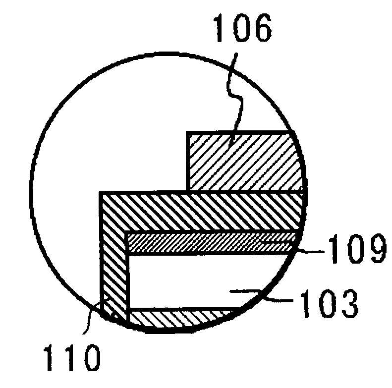
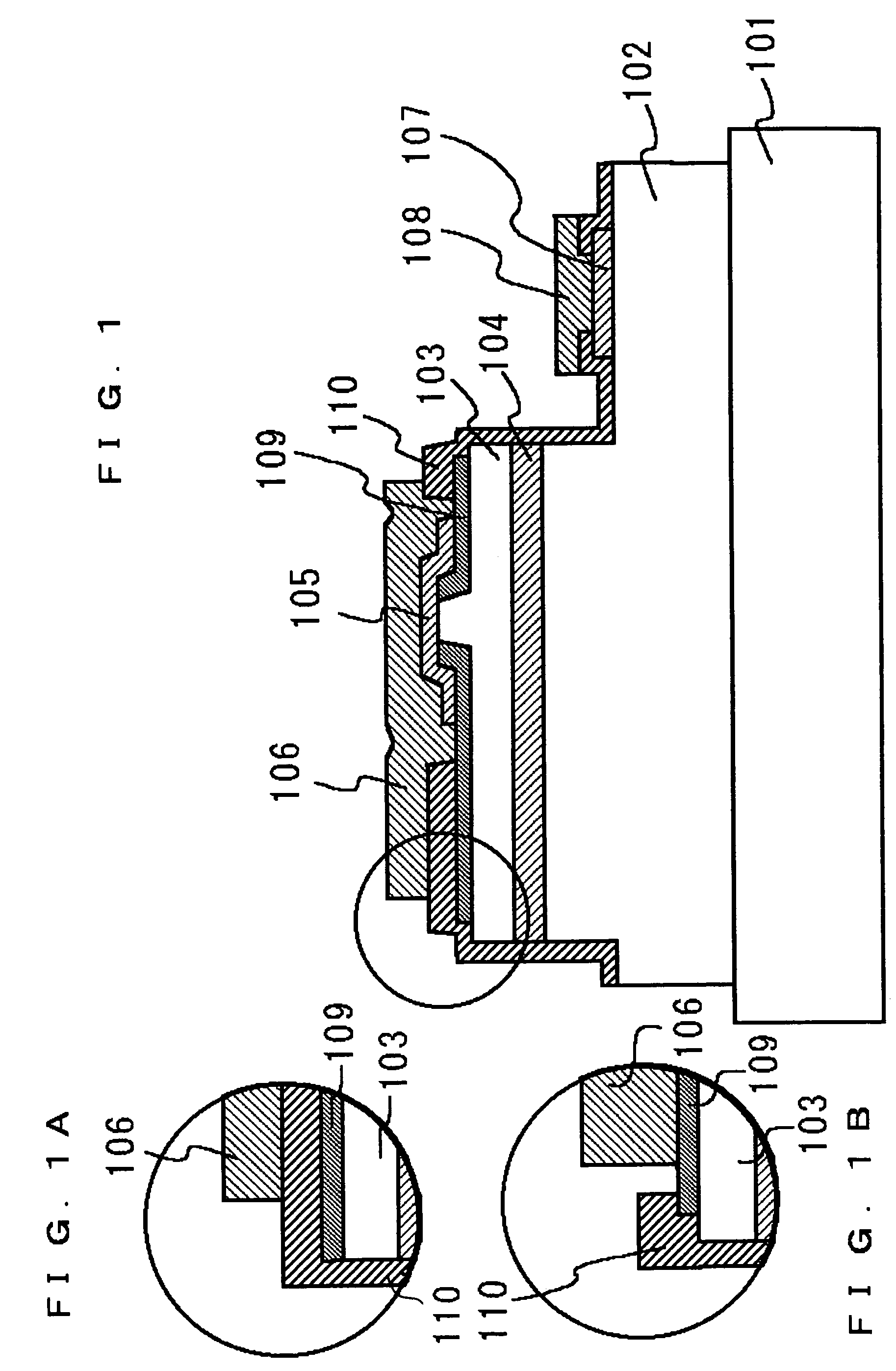
[0071]FIG. 1 shows a nitride semiconductor device according to a first embodiment. The nitride semiconductor device is a semiconductor laser diode (LD) including an n-type nitride semiconductor layer 102, an active layer 104, and a p-type nitride semiconductor layer 103 deposited in that order on a substrate 101. The p-type nitride semiconductor layer 103 has a ridge stripe. The ridge stripe is formed by partially etching the p-type nitride semiconductor layer or other processes to function as an effective refractive-index waveguide. Alternatively, the ridge stripe may be formed by partially etching a region from the p-type semiconductor layer to the n-type nitride semiconductor layer to function as a real refractive-index waveguide, or by the selective growth method. The ridge stripe is not necessarily formed in a mesa manner shape, in which the width of the stripe is gradually reduced upward. For example, it may be in a reversed mesa manner, in which the width is reduced downward,...

second embodiment

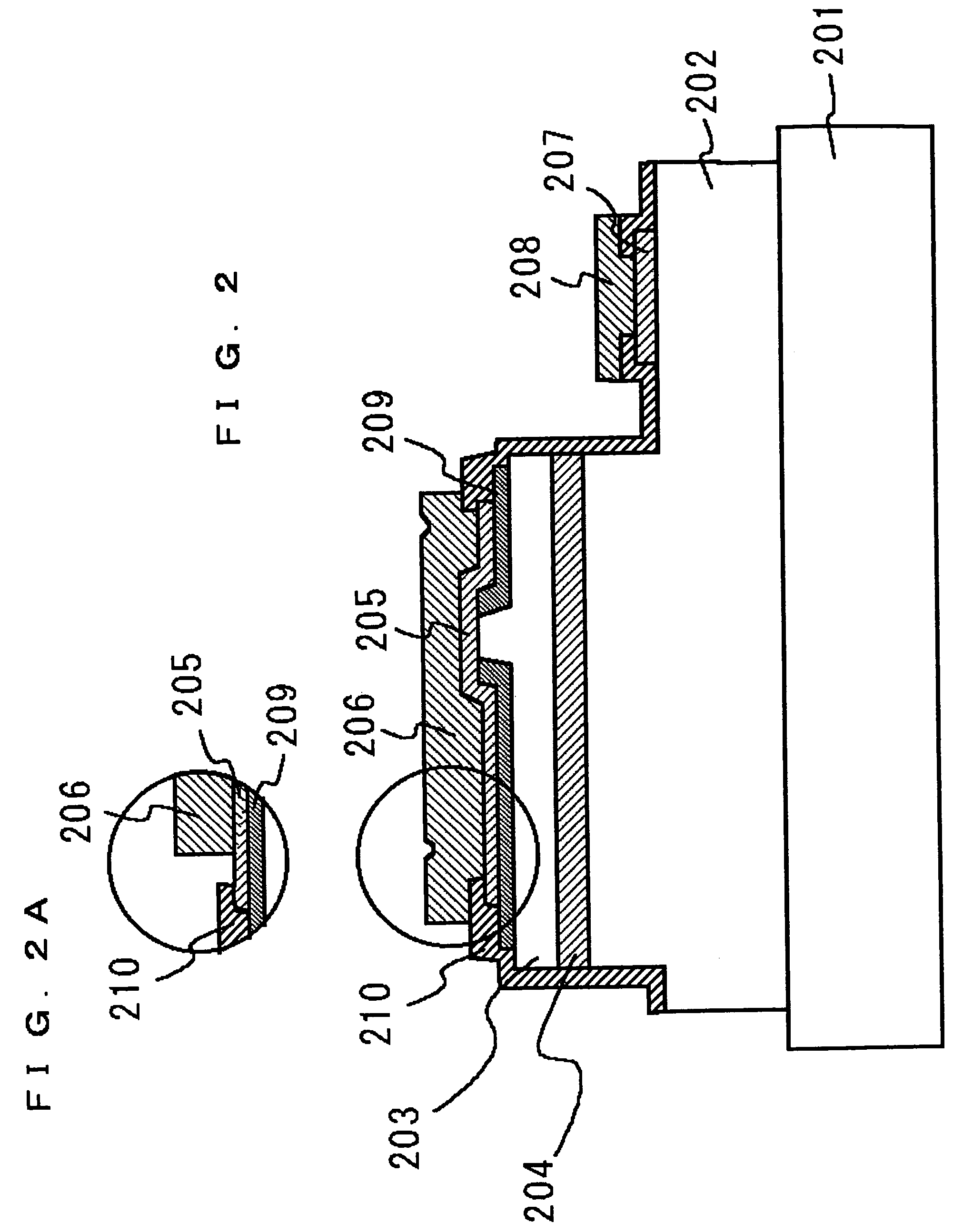
[0081]FIG. 2 shows a nitride semiconductor device according to a second embodiment of the present invention. The nitride semiconductor device is a semiconductor laser diode (LD) including an n-type nitride semiconductor layer 202, an active layer 204, and a p-type nitride semiconductor layer 203 deposited on a substrate 201, as in the first embodiment. The p-type nitride semiconductor layer 203 has a ridge stripe. A first p electrode 205 is formed so as to cover a wide region of a first insulating layer 209. A second insulating layer 210 is formed so as to overlap the first p electrode 205 in regions apart from the ridge stripe. A second p electrode 206 is formed on the first p electrode 205 and the second insulating layer 210. Hence, in second embodiment, the second p electrode 206 is not in contact with the first insulating layer 209. The light confinement in the waveguide region may be varied depending on the depth (height) of the ridge stripe of the first insulating layer 209, a...

third embodiment

[0083]FIG. 3 shows a nitride semiconductor device according to a third embodiment of the present invention. This nitride semiconductor device is a semiconductor laser diode (LD) including an n-type nitride semiconductor layer 302, an active layer 304, and a p-type nitride semiconductor layer 303 deposited on a substrate 301, as in the first embodiment. The p-type nitride semiconductor layer 303 has a ridge stripe. In the third embodiment, an adhesion layer 311 is provided between a second p electrode 306 and at least one of a first insulating layer 309 and a second insulating layer 310. The adhesion layer 311 increases the adhesion between the second p electrode 306 and the first insulating layer 309 or the second insulating layer 310, and is not placed on the upper surface of the ridge stripe, where a first p electrode 305 is joined to the second p electrode 306, or the vicinity of the upper surface.

[0084]The electrodes and insulating layers must have good adhesiveness not only to ...


PUM


Abstract

A nitride semiconductor device includes a semiconductor layer, a first electrode for establishing an ohmic contact disposed on the semiconductor layer, and a second electrode on the first electrode, having a different shape from that of the first electrode. A joint region is formed with the upper layer of the first electrode and the lower layer of the second electrode. The joint region comprises an element of the platinum group.

Description

BACKGROUND OF THE INVENTION[0001]1. Field of the Invention[0002]The present invention relates to semiconductor devices having micro-area (width) electrodes on nitride semiconductor layers, and particularly to high-current-driven electronic devices, such as laser diodes, high-power LEDs, FETs, and high-frequency devices. Such semiconductor devices comprise, for example, group III–V nitride semiconductors, such as GaN, AlN, and InN, including their mixed crystals AlGaN, InGaN, and AlInGa.[0003]2. Discussion of the Related Art[0004]Nitride semiconductor devices emit light having a wide range of wavelengths from a relatively short-wavelength ultraviolet region to a visible light region including that of red light, and are widely used for semiconductor laser diodes (LDs) and light emitting diodes (LEDs). The nitride semiconductor devices have been developed to increase miniaturization, increase lifetime, and enhance power. These devices have been principally used in electronic devices su...

Claims


Application Information

Patent Timeline
IPC IPC(8): H01L33/00H01L21/285H01L29/20H01L29/45H01L33/32H01L33/38H01L33/40
CPCH01L21/28575H01L29/452H01L33/40H01S5/0425H01L33/38H01L29/2003H01L33/32H01S5/22H01L33/387H01S5/32341H01S2301/176H01S5/04252H01S5/04254B42D1/08B42F5/00
Inventor SUGIMOTO, YASUNOBUYONEDA, AKINORI
Owner NICHIA CORP
Why Eureka
Try Eureka