Non-volatile memory architecture to improve read performance

a non-volatile memory and read performance technology, applied in static storage, digital storage, instruments, etc., can solve the problems of increasing signal development time, parasitic capacitances, and large array sizes, and achieve the effect of improving read performan

Active Publication Date: 2006-03-07
INTEGRATED SILICON SOLUTION
View PDF9 Cites 29 Cited by
  • Summary
  • Abstract
  • Description
  • Claims
  • Application Information

AI Technical Summary

Benefits of technology

[0014]The present invention provides a memory array with read circuitry for improved read performance. In one embodiment, the memory array is divided into an even number of sectors, where each sector is further divided into groups of memory cells and the groups divided into sub-groups. Thus, each sub-group contains an array of memory cells, which may be nonvolatile, flash EPROM, and EEPROM, among others. Each pair of sectors shares the same read circuitry, which includes multiplexers connected to bit lines and local sense amplifiers receiving the output of the multiplexers.
[0017]The total sense time needed for a read operation is the sum of the time for a sensing current to charge or discharge the associated bit lines (local sense amplifiers) and the time for a sensing current to charge or discharge the data line (global sense amplifiers). The total sense time can be reduced, according to the present invention, by increasing the sensing current for the global sense amplifiers. This can be accomplished by increasing the size of the local sense amplifiers, which may lie along a periphery of the device. Further, the groups and sub-groups may be divided into larger or smaller groups to change the granularity of the memory array. Finer granularity of the first stage sense amplifier makes it possible to use bit line multiplexers of narrower width which in turn allows simpler single stage multiplexer design with smaller parasitic capacitance.
[0018]The present invention also provides a better matching of bit line loading. In a read operation, the bit line in the opposite sector at the same column location is used as a reference bit line. The opposite sector is not enabled for read operation. The reference bit line is selected by the corresponding multiplexer and used as a reference by the local sense amplifier for the selected bit line coupled to the memory cell to be read. Since the reference signal is received from circuitry that is the same and in the same symmetric location as the selected signal, mismatches caused by dummy elements being located away from the active elements are greatly reduced. In another aspect, the reference cell current can be generated globally, such as by a circuit along the array periphery, and mirrored from the current source into the array.

Problems solved by technology

Thus, as memory arrays become larger, the bit-lines become longer and the bit line multiplexers become wider, resulting in larger parasitic capacitances.
This in turn increases signal development time.
Higher density results in larger array size and in turn larger parasitic capacitances.
Another disadvantage with such a divided bit line scheme is that of a mismatch in capacitance loading between a regular bit line and a reference bit line.
Consequently, the mismatch of capacitance loading between the dummy bit line multiplexer and the regular bit line multiplexer is increased.
This mismatch reduces the read performance of the array by increasing read time to maintain the same level of accuracy.
Building a reference bit line and reference bit line multiplexer with identical layout and parasitic capacitances to those of a regular bit line and bit line multiplexer is very costly and / or greatly increases the array size to the extent that such an option is not practical.

Method used


Image

  • Non-volatile memory architecture to improve read performance
  • Non-volatile memory architecture to improve read performance
  • Non-volatile memory architecture to improve read performance

Examples


Embodiment Construction

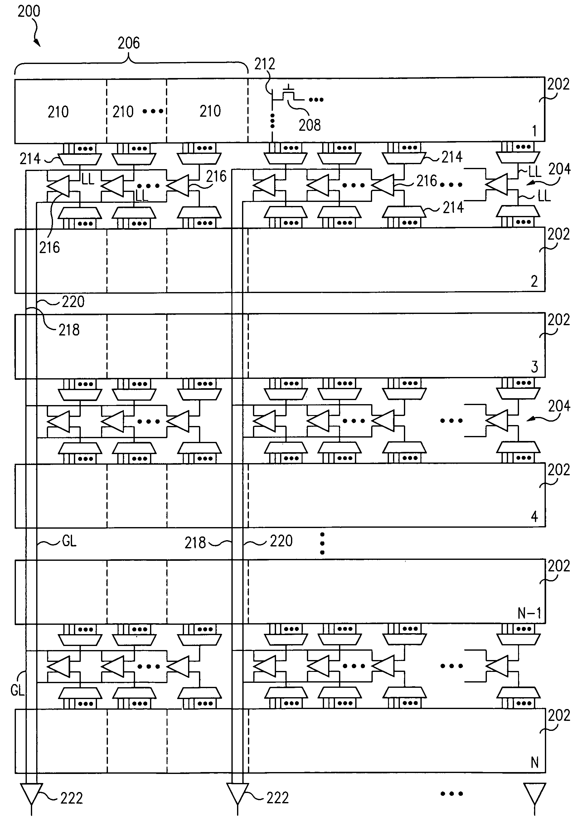
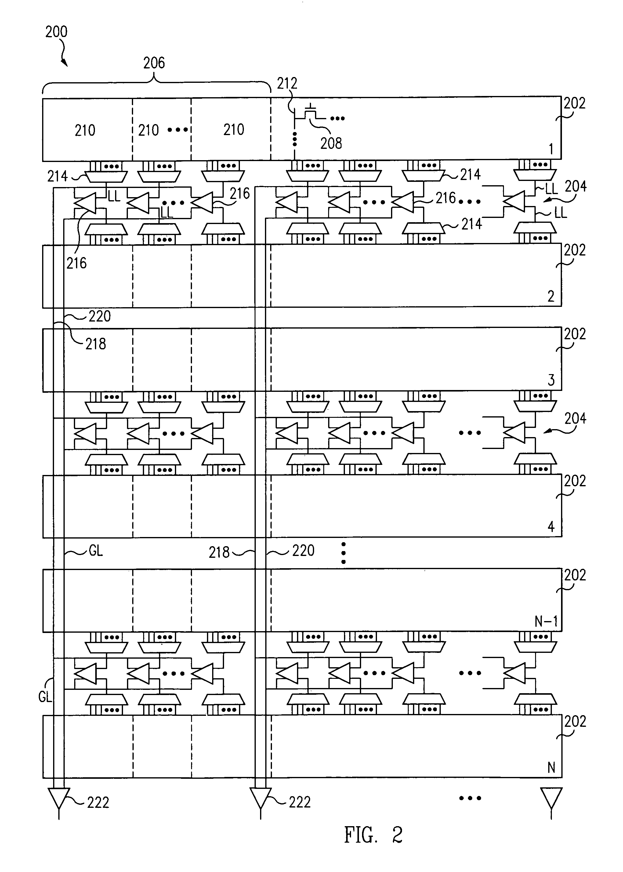
[0023]According to one aspect of the present invention, a memory cell array is physically divided into an even number of sectors, with each pair of sectors having local read circuitry comprising local sense amplifiers and multiplexers. Each sector is divided into groups of memory cells, with each group further divided into sub-groups of memory cells. Each sub-group is associated with a multiplexer and a local sense amplifier, with the sense amplifier being shared with another sub-group from a corresponding sector. A global sense amplifier is associated with each group of memory cells and local sense amplifiers. The local sense amplifiers sense local data lines within the sectors, while the global sense amplifiers sense global data lines associated with each group of memory cells. Thus, a two-stage sensing scheme is employed.

[0024]The present invention also takes advantage of physical space outside the memory array. Consequently, the transistor size of local sense amplifiers can be p...


PUM


Abstract

A memory cell array is physically divided into an even number of sectors, with each pair of sectors sharing read circuitry. The outputs of the shared read circuitry are commonly connected to form data lines spanning the height of the array, which are input to global sense amplifiers. A two-stage sensing scheme is employed, with first stage and global sense amplifiers. The driving capability of the first stage sense amplifier can be used to decrease the time to charge or discharge the data lines, which reduces the total signal development time and consequently improves read performance. Granularity of the array can be adjusted by dividing groups and sub-groups of memory cells within a sector accordingly. In a read operation, the bit line in the opposite sector at the same column location is used as reference bit line, which greatly improves matching of bit line loading for the sensing.

Description

BACKGROUND[0001]1. Field of the Invention[0002]The present invention relates generally to semiconductor memory devices, and more particularly to read architectures for non-volatile memories.[0003]2. Related Art[0004]Non-volatile semiconductor memories and arrays are widely used to store written or programmed information or data. The information or data, represented as a “1” or “0”, is stored in individual memory cells, such as EEPROMs, EPROMs, NOR-type flash memory cells, or NAND cells. An array of such individual memory cells are interconnected by columns of bit lines and rows of word lines. Associated bit-line and word-line decoders allow specific memory cells to be accessed or read, erased, and programmed by applying appropriate voltages to selected bit lines and word lines. In a typical read operation, a read circuit senses the threshold voltage of a floating gate transistor in a memory cell to determine the value or data stored in the cell. The sensing can be with a conventiona...

Claims


Application Information

Patent Timeline
Patent Type & Authority Patents(United States)
IPC IPC(8): G11C16/00
CPCG11C16/26
Inventor LIU, KER-CHING
Owner INTEGRATED SILICON SOLUTION
Why Eureka
Try Eureka