Differential drive semiconductor optical modulator

a technology of semiconductor optical modulator and drive chip, which is applied in the direction of optical waveguide light guide, instruments, optics, etc., can solve the problems of power consumption and voltage use efficiency drawback, difficult to manufacture such a modulator and achieve sufficient performance, etc., to achieve the effect of enhancing modulation bandwidth and reducing power consumption

Active Publication Date: 2006-03-07
MITSUBISHI ELECTRIC CORP
View PDF4 Cites 9 Cited by
  • Summary
  • Abstract
  • Description
  • Claims
  • Application Information

AI Technical Summary

Benefits of technology

[0030]According to the present invention, in a differential driving system of semiconductor modulators, differential signals are transferred along transmission lines and additive inductance is provided in the output side of each semiconductor modulator, thereby compensating narrowing of bandwidth due to junction capacitance of each semiconductor modulator. Consequently, an appropriate optical modulation waveform with a higher extinction ratio can be attained, resulting in remarkable enhancement of modulation bandwidth.

Problems solved by technology

However, since only one of two differential outputs is utilized for a driving signal and another of differential outputs is not utilized, resulting in a drawback in respect of power consumption and voltage use efficiency.
However, it is difficult to manufacture such a modulator and attain a sufficient performance since the manufacturing process is super-fine.

Method used


Image

  • Differential drive semiconductor optical modulator
  • Differential drive semiconductor optical modulator
  • Differential drive semiconductor optical modulator

Examples


embodiment 1

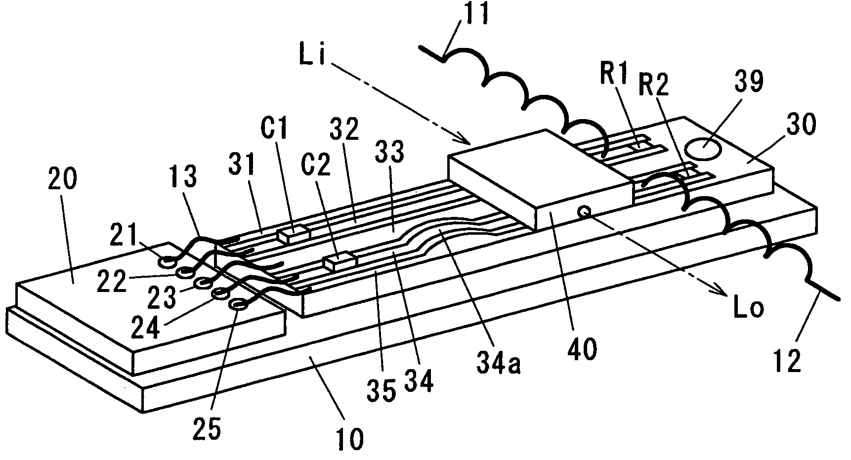
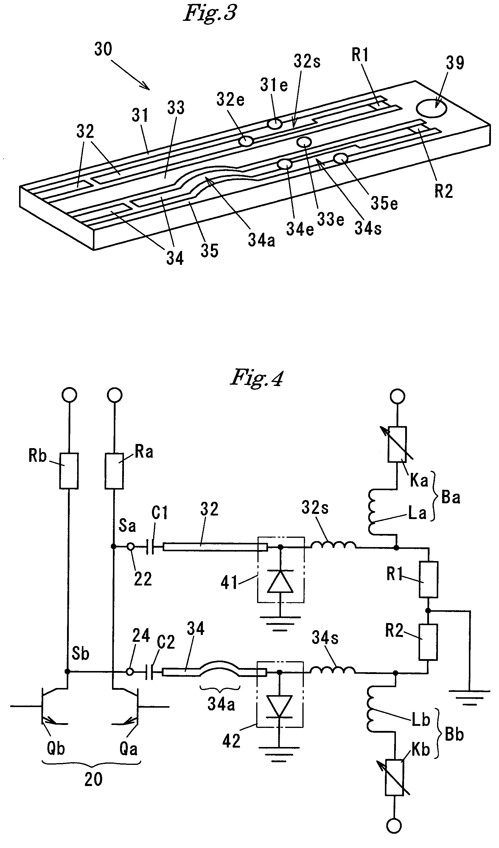
[0046]FIG. 1 is a perspective view showing a first embodiment of the-present invention. A differential drive type semiconductor optical modulator includes a chip carrier 10, a differential driver circuit 20 mounted on the chip carrier 10, a transmission-line substrate 30 mounted on the chip carrier 10, and a optical modulator integrated device 40 mounted on the transmission-line substrate 30.

[0047]The chip carrier 10 is formed in a rectangle shape of a conductive material, such as metals, or an electrically insulating material, such as ceramics, to serve as a base of the whole optical modulator.

[0048]The differential driver circuit 20 serves to output a pair of differential signals Sa and Sb for driving the optical modulator integrated device 40 based on a modulation signal from an external circuit. The circuit 20 is constituted of an integrated circuit in which a number of transistors are integrated on an substrate of, e.g. InP, which is mounted on the chip carrier 10 by die bondin...

embodiment 2

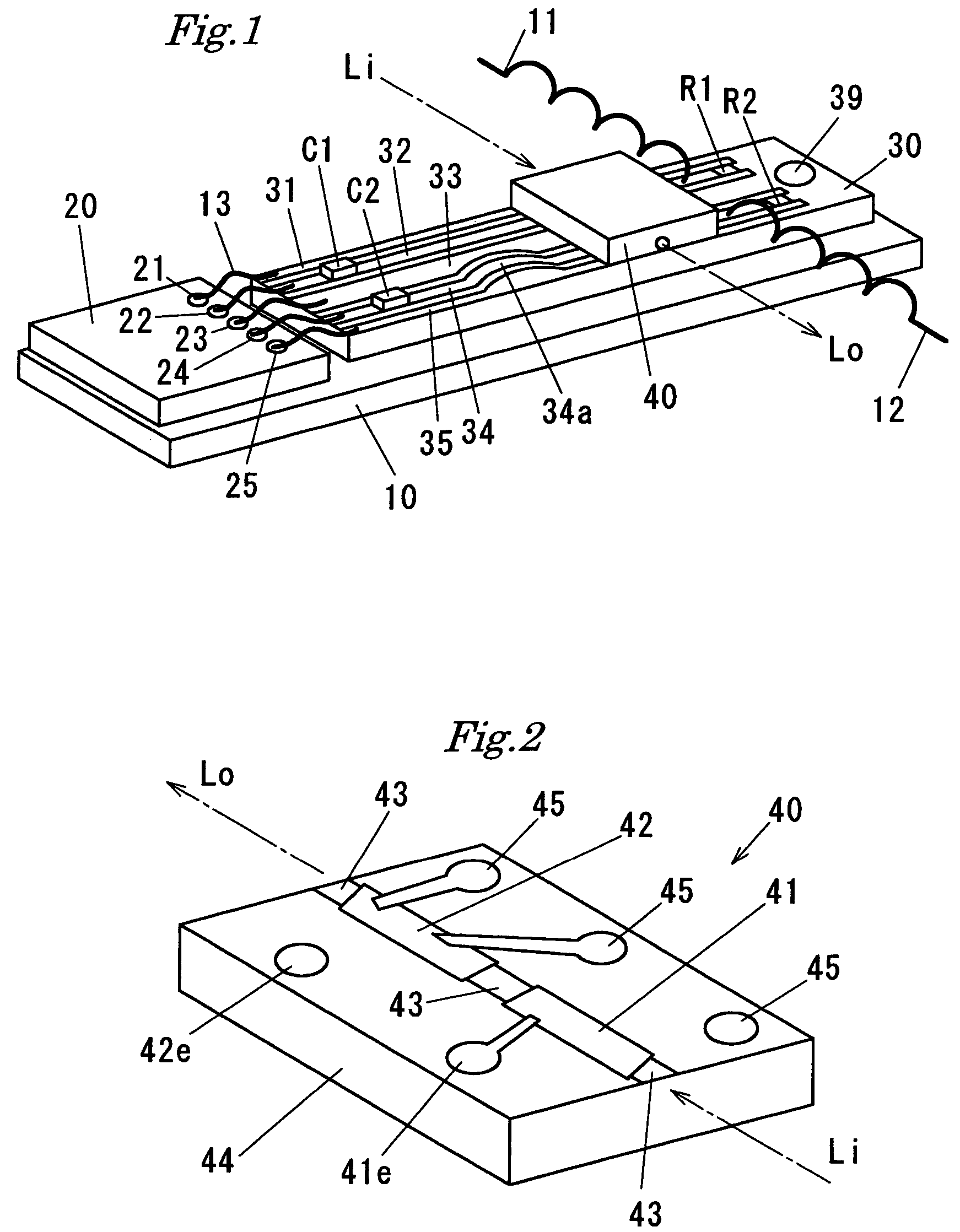
[0099]FIG. 6 is a perspective view showing a second embodiment of the present invention. A differential drive type semiconductor optical modulator includes a chip carrier 10, a differential driver circuit 20 mounted on the chip carrier 10, a transmission-line substrate 30 mounted on the chip carrier 10, a optical modulator integrated device 40 mounted on the transmission-line substrate 30, and a phase inverter 50 for inverting phase of an electric signal by 180 degrees.

[0100]The chip carrier 10, the differential driver circuit 20 and the transmission-line substrate 30 are similar to those of FIG. 1, so redundant descriptions will be omitted here.

[0101]The optical modulator integrated device 40 is a chip in the shape of a rectangular parallelepiped which has been cut away from a semiconductor wafer, which includes semiconductor modulators 41 and 42 arranged in series along a common optic axis, and an optical waveguide 43 for optically connecting the semiconductor modulators 41 and 42...


PUM

PropertyMeasurementUnit
impedanceaaaaaaaaaa
dielectric constantaaaaaaaaaa
cutoff frequencyaaaaaaaaaa

Abstract

A differential drive semiconductor optical modulator includes: a differential driver circuit having output pads which can output a pair of differential signals; a transmission-line substrate having transmission lines connected to the output pads and ground lines; and semiconductor modulators mounted on the transmission-line substrate, arranged in series along a common optical axis; terminal resistors connected to terminal ends of the transmission lines and inductances interposed between the semiconductor modulators and the terminal resistors, on the transmission-line substrate, producing an appropriate optical modulation waveform with a high extinction ratio and enhanced modulation bandwidth.

Description

BACKGROUND OF THE INVENTION[0001]1. Field of the Invention[0002]The present invention relates to a differential drive semiconductor optical modulator, which is suitable for an optical modulator in optical transmission systems.[0003]2. Description of the Related Art[0004]In optical transmission systems, a optical modulator for modulating light based on an electric signal is used, and the signal transmission capacity can be improved by enhancing the modulation rate thereof.[0005]The related prior arts are listed as follows:[0006][document 1] U.S. Pat. No. 5,930,022[0007][document 2] Japanese Patent Unexamined Publications (koukai): JP-2002-277840, A[0008][document 3] Japanese Patent Unexamined Publications (koukai): JP-2002-296552, A[0009][document 4] Hiroaki Takeuchi et al., “High-speed Electroabsorption Modulators with Traveling-Wave Electrodes”, OFC2002 Technical Digest WV1, 2002[0010]The document 1 discloses an example where a differential amplifier is employed for a driver circui...

Claims


Application Information

Patent Timeline
Patent Type & Authority Patents(United States)
IPC IPC(8): G02F1/01G02B6/12G02F1/03G02F1/035G02F1/015G02F1/025
CPCG02F1/025G02F1/0121
Inventor HATTA, TATSUOOKADA, NORIO
Owner MITSUBISHI ELECTRIC CORP
Why Eureka
Try Eureka