Combinational circuit, and encoder, decoder and semiconductor device using this combinational circuit

a combinational circuit and encoder technology, applied in the field of combinatorial circuits, can solve the problems of increasing the inappropriateness of the conventional method of low-speed serial reed-solomon decoders arranged in parallel, reducing the processing speed, and reducing the processing cos

Inactive Publication Date: 2006-03-07
INT BUSINESS MASCH CORP
View PDF3 Cites 15 Cited by
  • Summary
  • Abstract
  • Description
  • Claims
  • Application Information

AI Technical Summary

Benefits of technology

[0113]TABLE 2VariableCross-termResiduepre-processgenerationoperationStandard AND-XORNone+64AND+103XORmultiplication circuitComposite Field Multiplier 4XOR*2+48AND +56XORXOR-AND-XOR circuit for performing the multiplication of sub-extension field GF(24) to obtain the effects of the inventiona. Alteration of all three22XOR*2+30AND+44XORmultiplications of asub-fieldb. Alteration of two out16XOR*2+36AND+48XORof three multiplicationsc. Alteration of one of10XOR*2+42AND+52XORthree multiplications
[0114]Multiplier Structure for a Combinational Circuit According to the Invention
[0115]Generally, optimization of Boolean algebra is difficult when many multiplications and logical sum calculations are performed together. However, in consideration of the use of the combinational circuit as the processor 12 for the invention, many logical sum calculators and many multipliers are connected in parallel at multiple stages. The i-th logical sum calculator generally receives 0-th to (i−1)th outputs. Therefore, since the backend part of the operation circuit must process in parallel inputs used in common by almost the entire combinational circuit, the optimization range is extended. The present inventors focused on this point, and achieved an efficient configuration for a multiplier by performing the optimization for Boolean algebra, while taking into account the balance obtained with other operations.
[0116]FIG. 10 is a diagram showing a combinational circuit according to the embodiment wherein a three-stage structure is employed for the multiplier in the combinational circuit in FIG. 7, which includes conventional multipliers and adders. In the combinational circuit in FIG. 10, an input A1 is transmitted to a first XOR group 52, an input B1 is transmitted to a second XOR group 54, and an input B2 is transmitted to a third XOR group 56. These XOR groups 52, 54 and 56 are gates used by this invention to perform the variable pre-process. Since the XOR groups 52 process the common input A1, the circuit size is reduced. The outputs of the XOR groups 52, 54 and 56 are transmitted to AND groups 58, and when a cross-term is obtained, the residue operation is performed again by downstream XOR groups 60, an output 62 being generated by an XOR group 60a, and an output 64 being generated by an XOR group 60b. In FIG. 10, the unit for performing one multiplication is indicated by broken line BL, and three stages, a variable pre-processor (XOR)—a cross-term operation unit (AND)—a residue operation (XOR), constitute one multiplier. As is shown in FIG. 10, when the XOR-AND-XOR structure is employed for each multiplier, and when for the multipliers the XOR calculations to be performed for an input used in common is unified, the XOR calculation circuits can be shared by the multipliers. So long as the size of a portion (variable pre-processors*2+new cross-term generation+new residue operation unit) that corresponds to one multiplier is the same or slightly larger than the normal multiplication circuit, the size of the entire multiplier group can be reduced.
[0117]FIG. 11 is a diagram showing a combinational circuit according to another embodiment wherein a three-stage multiplier used for the invention is mounted for the conventional combinational circuit in FIG. 10. In the combinational circuit in FIG. 11, inputs 66, 68, 70 and 72 are transmitted to XOR groups 74, 76, 77 and 78 that perform the variable pre-process, and the outputs of the individual XOR groups are transmitted to AND groups 80 and 82 that perform the cross-term generation operation.
[0118]The outputs of the AND groups 80 and 82 are transmitted to an addition circuit 84 and are added together, and the residue operation and the multiplication are again performed by a backend XOR group 86 that is used in common, so that an output 88 is generated. The structure of one multiplier in FIG. 11 is formed in a block Bx. The difference from the structure in FIG. 10 is that, in the invention, even when the XOR groups 74, 76, 77 and 78 on the input side are not shared the backend or output side XOR group 86 that performs the residue operation is used in common.

Problems solved by technology

However, the decoding circuit in FIG. 1 can not provide a processing speed that equals 40 Gbps required for optical communication, and in order to cope with the 8-byte error correction standard established by the ITU, when the normal circuit sharing method is used the resulting circuit can be so large that it can not be mounted on a single chip.
With this configuration, as the communication speed of an optical communication field increases, the conventional method whereby low-speed serial Reed-Solomon decoders are arranged in parallel becomes ever more inappropriate.
This is a critical path that prevents an increase in output speed, and the processing speed can not be satisfactorily increased.
According to OC-768 SONET, this is a large problem, because assuming the 16 interleave defined by ITU-G709 is employed as an input / output interface for the decoding circuit, a fast processing speed of 300 MHz or higher is expected.
However, even when the process is converted into a pipeline, the decoding circuit in FIG. 4 must perform divisions at locations whereat no error is present, and the circuit size and the power consumption are increased as the pipeline is constructed.
Further, to perform divisions only for error locations, the locations must be calculated in advance, so that the error locations and the error values can not be calculated in parallel.
Therefore, when a synchronous frame, such as SONET, for sequential data must be input or output at high speed, it is difficult to output error values at high speed for a constant cycle, without depending on error patterns (number of errors and their locations).
However, for interleaved Reed-Solomon codes, as defined by ITU-T G.975, since signals must be rearranged using a large, high-speed buffer and selector, the parallel Reed-Solomon decoding method is not always efficient.
Therefore, it is difficult for the parallel Reed-Solomon decoding method to he provided at a practical level for optical communication.
As one of various reasons this has not been done, it may be presumed many decoding operations tend to be performed by sequential circuits, and it has been ascertained that the use of a combinational circuit provides little merit in terms of processing capabilities and an acceptable circuit size.
When the algorithm for solving the Yule-Walker equation is performed by a combinational circuit to achieve high-speed processing, in as the required error correction capabilities increase, the portion of the circuit used to solve the Yule-Walker equation and to locate errors becomes very significant from the viewpoint of the reduction in the size of the combinational circuit.

Method used


Image

  • Combinational circuit, and encoder, decoder and semiconductor device using this combinational circuit
  • Combinational circuit, and encoder, decoder and semiconductor device using this combinational circuit
  • Combinational circuit, and encoder, decoder and semiconductor device using this combinational circuit

Examples


Embodiment Construction

[0066]The preferred embodiment of the present invention will now be described by referring to the accompanying drawings. Note, however, that the present invention is not limited to this embodiment.

[0067]Section 1 Decoding Circuit

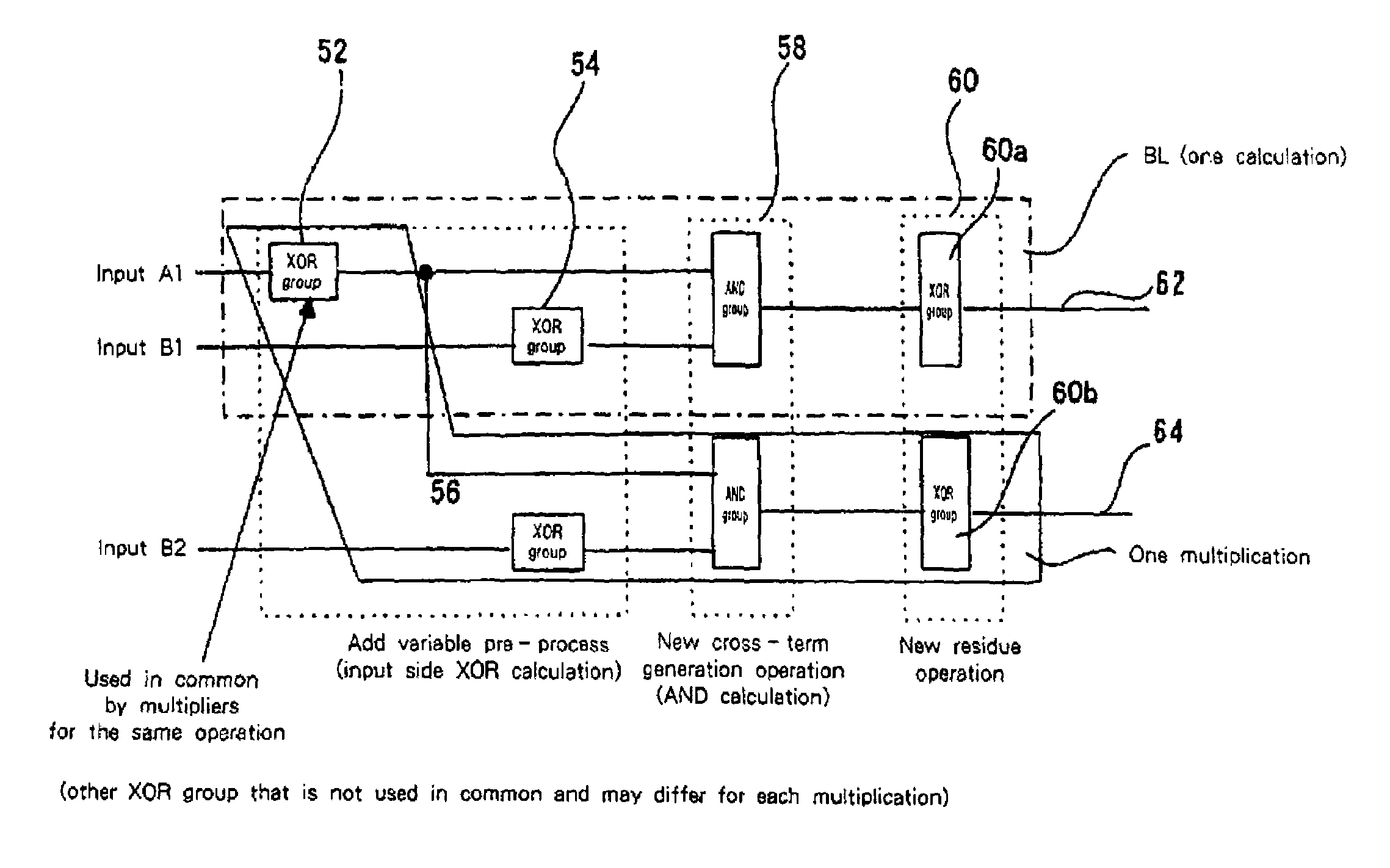
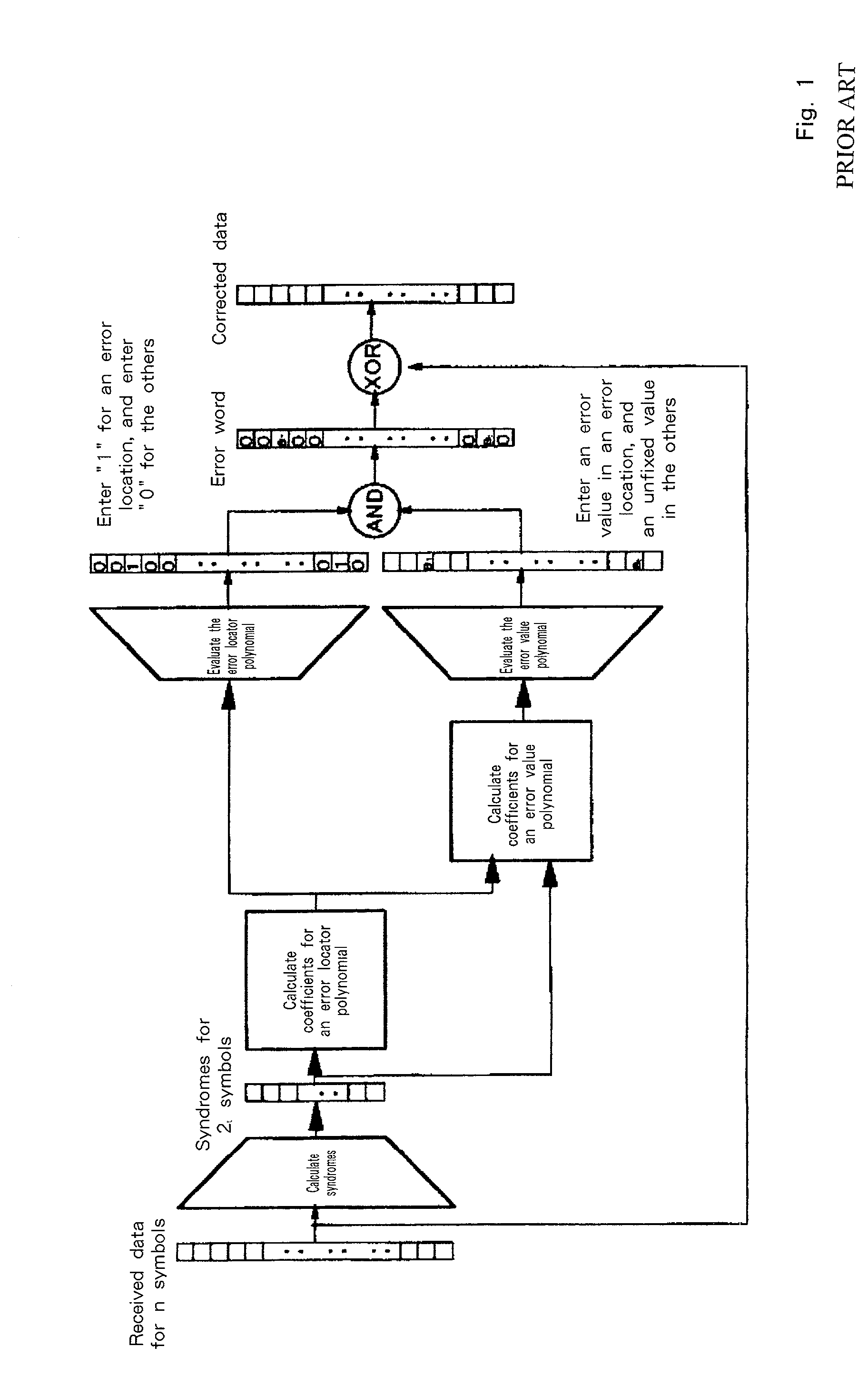
[0068]FIG. 6 is a diagram showing a decoder according to the present invention that can be used to correct errors in digital signals received through optical communication. The decoder in FIG. 6 includes an input unit 10, a processor 12 and an output unit 14. The input unit 10 receives a 16-byte interleaved digital signal ID. The processor 12 processes a signal received from the input unit 10 and calculates coefficients of an error locator polynomial and coefficients of an error value polynomial. And the output unit 14 obtains an AND of the Λ(x) evaluation result and Er(x) evaluation result that are generated from the data received from the processor 12, performs an XOR process with the AND result and the input digital signal ID, and generates a digital sign...


PUM


Abstract

A combinational circuit comprises: a plurality of multipliers, independently performing two or more multiplications for coded digital signals in a Galois extension field GF(2m) (m is an integer equal to or greater than 2), wherein the multipliers include an input side XOR calculator, an AND calculator, and an output side XOR calculator, and wherein the multipliers share the input side XOR calculator. Further, according to the present invention, these multipliers each include an adder connected between an AND calculator and an output side XOR calculator, wherein the output side XOR calculator is used in common, and wherein the outputs of the AND calculators in the multipliers are added by the adders, and the addition results are calculated by the output side XOR calculator that is used in common.

Description

BACKGROUND OF THE INVENTION[0001]1. Field of the Invention[0002]The present invention relates to a combinational circuit, and an encoder, a decoder and a semiconductor device that use this combinational circuit. More specifically, the present invention relates to a combinational circuit that can effectively correct errors, especially in a fast optical communication field, and an encoder, a decoder and a semiconductor device that use this combinational circuit.[0003]2. Brief Description of the Prior Art[0004]Importance of Fast and Superior Error Correction Technique[0005]In consonance with the expansion of the Internet and the development of e-business, the rate of increase in the volume of data computers can handle and their speed has accelerated. Accordingly, there is a demand for increasing speed of data transfer among computers, and in line with this demand, optical communication that yields transfer speed of up to 40 Gbps is becoming popular. However, for such a fast communicati...

Claims


Application Information

Patent Timeline
Patent Type & Authority Patents(United States)
IPC IPC(8): H03M13/00G06F11/10H03M13/15H03M13/37
CPCH03M13/1515H03M13/1525H03M13/6502H03M13/158H03M13/37H03M13/1555
Inventor MORIOKA, SUMIOKATAYAMA, YASUNAOYAMANE, TOSHIYUKI
Owner INT BUSINESS MASCH CORP
Why Eureka
Try Eureka