Method for forming thin film and method for fabricating liquid crystal display using the same

a liquid crystal display and thin film technology, applied in the field of thin film forming, can solve the problems of increasing the resistivity of copper film, complicated whole process, and requiring additional complicated processes,

Inactive Publication Date: 2006-03-14
LG DISPLAY CO LTD
View PDF5 Cites 50 Cited by
  • Summary
  • Abstract
  • Description
  • Claims
  • Application Information

AI Technical Summary

Benefits of technology

[0020]An object of the invention is to solve at least the above problems and/

Problems solved by technology

These methods have a problem in that a wet chemical process is required, and therefore additional complicated processes, such as removing, washing, and drying, are required.
This complicates the whole process.
First, in case the metal, specifically copper, is formed by the

Method used


Image

  • Method for forming thin film and method for fabricating liquid crystal display using the same
  • Method for forming thin film and method for fabricating liquid crystal display using the same
  • Method for forming thin film and method for fabricating liquid crystal display using the same

Examples


Embodiment Construction

[0036]Reference will now be made in detail to the preferred embodiments of the present invention, examples of which are illustrated in the accompanying drawings.

[0037]A method for forming a thin film according to the present invention will be described with reference to FIGS. 2a–2c.

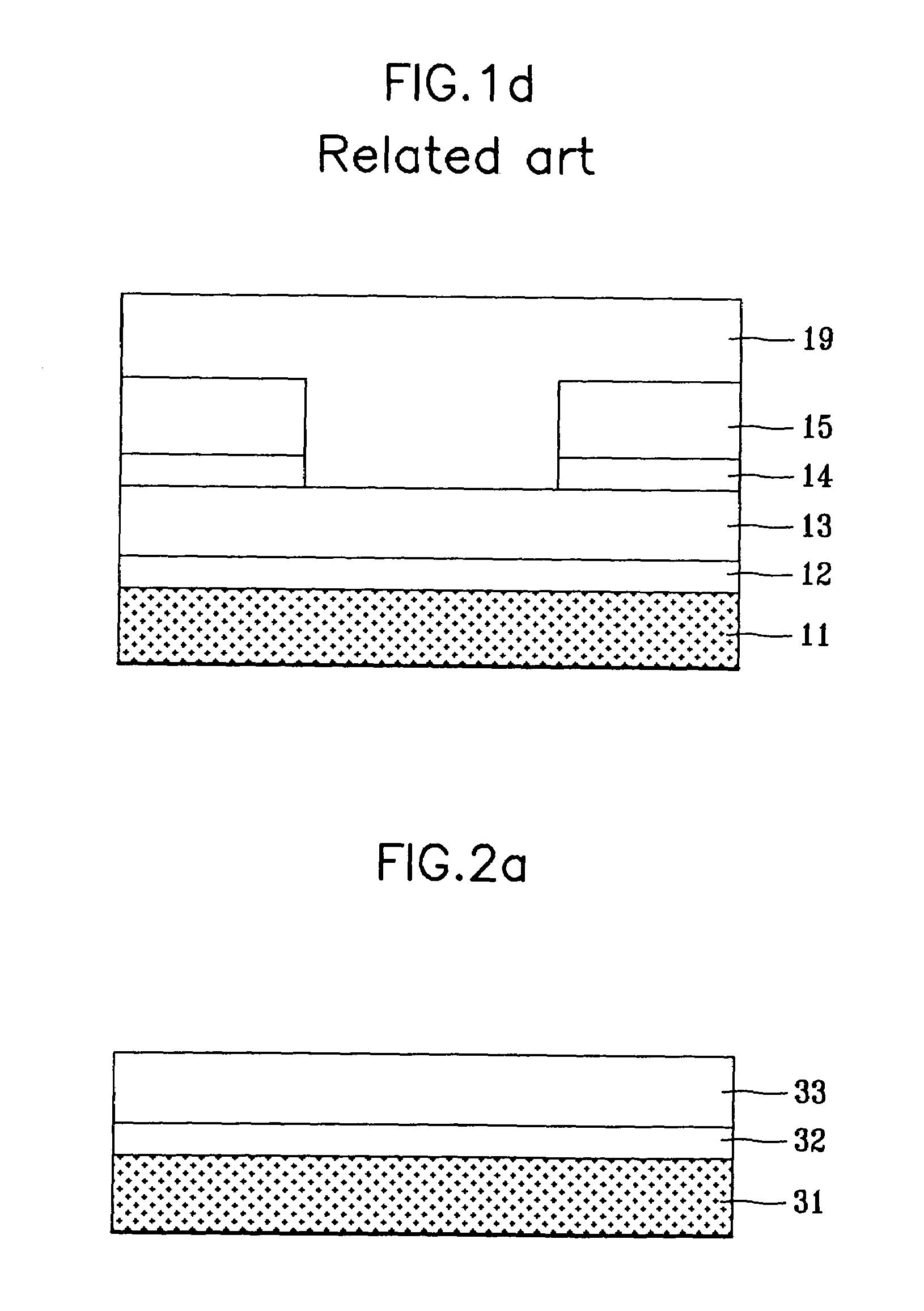
[0038]As shown in FIG. 2a, a diffusion barrier film 32 is formed on a substrate 31, and a seed layer 33 for growing copper is formed on the diffusion barrier film 32.

[0039]At this time, since the seed layer 33 is exposed to the air, a copper oxide film is formed on a surface of the seed layer 33.

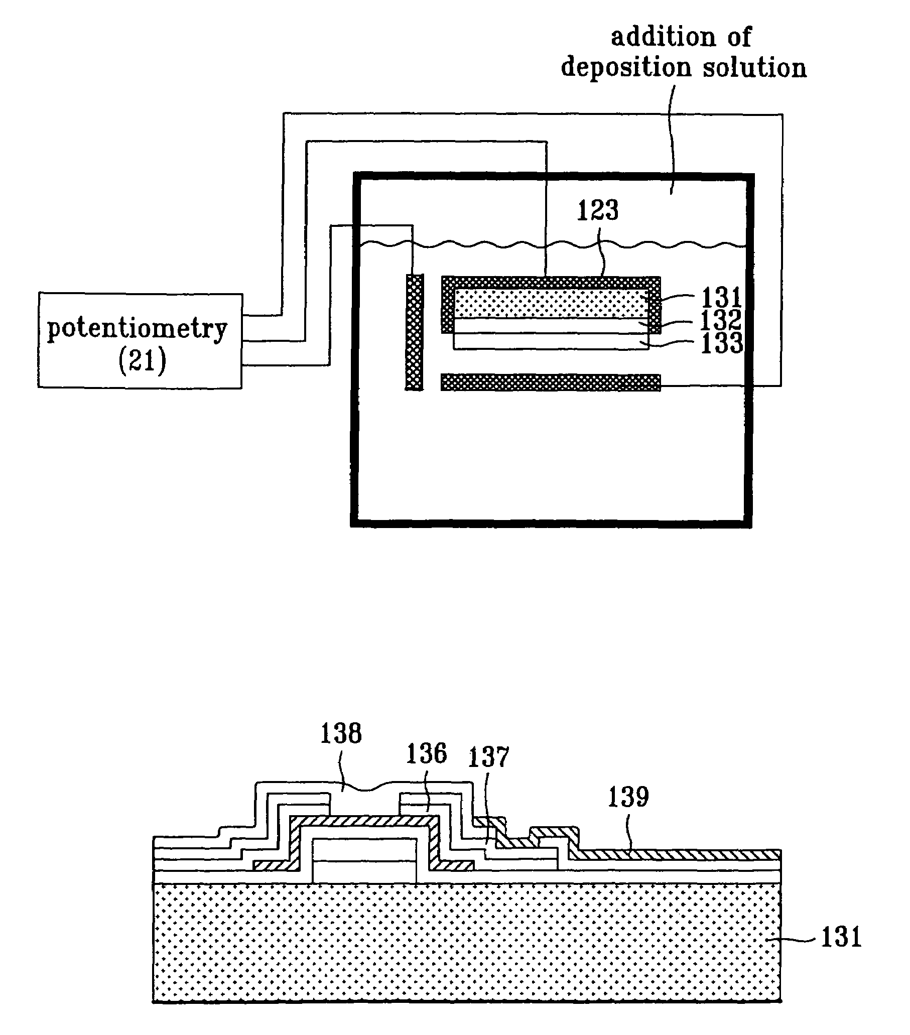
[0040]Subsequently, as shown in FIG. 2b, the substrate 31 is dipped in a tub 35 containing an electrolyte solution 36 with H2SO4 and H2O, so that the copper oxide film formed on the surface of the seed layer 31 is removed.

[0041]In the tub 35, there are a reference electrode 22, a working electrode 23, and a counter electrode 24 opposing the working electrode 23. The reference electrode 22, the working electrode 2...


PUM


Abstract

A method for forming a thin film and a method for fabricating a liquid crystal display device using the same are provided. The method provides a process that is simplified. Uniform thin film characteristics can be obtained. The method for forming a thin film includes the steps of forming a diffusion barrier film on a substrate, forming a metal seed layer on the diffusion barrier film, removing a metal oxide film formed on a surface of the metal seed layer using an electric plating method, and depositing metal on the metal seed layer in which the metal oxide film is removed.

Description

[0001]This application is a divisional of prior application Ser. No. 09 / 985,342, filed Nov. 2, 2001 now U.S. Pat. No. 6,706,628.[0002]This application claims the benefit of Korean Patent Application No. 2000-67200 filed on Nov. 13, 2000, which is hereby incorporated by reference as if fully set forth herein.BACKGROUND OF THE INVENTION[0003]1. Field of the Invention[0004]The present invention relates to a method for forming a thin film, and more particularly, to a method for forming a thin film and a method for fabricating a liquid crystal display device using the same, in which a process is simplified and uniform thin film characteristic can be obtained.[0005]2. Discussion of the Related Art[0006]Traditionally, an aluminum or its alloy has been used as a line material of a semiconductor device or a liquid crystal display device. Recently, there has been an increase in the use of copper having excellent electric conductivity as the line material in semiconductor device and liquid cry...

Claims


Application Information

Patent Timeline
IPC IPC(8): H01L21/00H01L21/3205H01L21/44H01L21/288G02F1/00H01L21/3213H01L21/336H01L21/768H01L29/45H01L29/49
CPCH01L21/2885H01L21/32134H01L21/76838H01L21/76852H01L29/66765H01L21/76873H01L29/458H01L29/4908H01L21/76861G02F1/00
Inventor KIM, SOO KILBAE, JONG UKKIM, JAE JEONG
Owner LG DISPLAY CO LTD
Why Eureka
Try Eureka