Plasma display device with shielding parts on transparent electrodes

a technology of transparent electrodes and display devices, which is applied in the direction of electrodes, gas-filled discharge tubes, discharge tubes/lamp details, etc., can solve the problems of increasing external light reflection, lowering reducing the brightness of the entire screen, so as to prevent a drop in the color purity of blue light and improve the bright room contrast ratio

Inactive Publication Date: 2006-03-14
HITACHI LTD
View PDF17 Cites 10 Cited by
  • Summary
  • Abstract
  • Description
  • Claims
  • Application Information

AI Technical Summary

Benefits of technology

[0020]It is an object of the present invention to improve the bright room contrast ratio of a plasma display panel. In particular, the object of the present invention is to improve the bright room contrast ratio of a plasma display panel of ALIS technology.
[0021]According to one of the aspects of the present invention, a plurality of discharge electrodes having transparent electrodes connected to bus electrodes are arranged on an inner side of a front substrate. The front substrate is provided on the side of the display-surface where discharge-generated light radiates out to the exterior. Shielding parts for shielding the incident light from exterior are formed on the transparent electrodes. Thus, the shielding parts reduce the surface reflection to improve the bright room contrast ratio.
[0022]According to another aspect of the present invention, a plurality of discharge electrodes having transparent electrodes, and capable of discharging between neighboring electrodes on both sides are arranged on the inner side of the front substrate. The transparent electrodes are connected to bus electrodes, respectively. That is, discharge at a discharge electrode occurs at one timing with the neighboring discharge electrode on one side, and at another timing with the discharge electrode on the other side. The front substrate is provided on the display-surface side where discharge-generated light radiates out to the exterior. Besides, shielding parts for shielding the incident light from exterior are formed along the front substrate. Therefore, even in the plasma display panel in which discharge can be made between neighboring discharge electrodes on both sides, the shielding parts reduce the surface reflection to improve the bright room contrast ratio.

Problems solved by technology

Consequently, the PDP 38 of ALIS technology had a problem that the external light reflection increases to lower the bright room contrast ratio.
Simply arranging an optical filter at the front, however, lowers the brightness of the entire screen.

Method used


Image

  • Plasma display device with shielding parts on transparent electrodes
  • Plasma display device with shielding parts on transparent electrodes
  • Plasma display device with shielding parts on transparent electrodes

Examples


first embodiment

[0048]FIG. 7 shows the essential parts of the plasma display panel in the present invention. The same elements as those described in the conventional art will be designated by identical reference numbers. Detailed description thereof will be omitted.

[0049]This embodiment is formed as a PDP 42 of ALIS technology, having a plurality of discharge electrodes 40 formed at regular intervals. Bus electrodes 44 constituting the discharge electrodes 40 have a configuration different from heretofore. The arrangement of transparent electrodes 18 constituting the discharge electrodes 40 and the arrangement of address electrodes 16 and ribs 24 are nearly the same as those of FIG. 4.

[0050]The bus electrodes 44 are formed broader at portions lying between the address electrodes 16 and the ribs 24, and slightly broader at portions facing the address electrodes 16. These broader portions form shielding parts 46 for shielding light incident from exterior. That is, in this embodiment, the shielding pa...

second embodiment

[0069]This embodiment can offer the same effects as those obtained from the second embodiment described above.

[0070]FIG. 13 shows the essential parts of a fourth embodiment of the plasma display panel in the present invention. The same elements as those described in the conventional art and in the second embodiment will be designated by identical reference numbers. Detailed description thereof will be omitted.

[0071]This embodiment is formed as a PDP 66 of ALIS technology, and differs from the second embodiment in the configuration and arranged positions of shielding parts 68. The other structure is identical to that of the second embodiment. The shielding parts 68 are formed on the sides with the bus electrode 58 of the opposing parts 56b. That is, the shielding parts 68 are formed at positions away from the regions with high luminescent intensity, where the opposing parts 56b face each other.

[0072]This embodiment can offer the same effects as those obtained from the second embodime...

fifth embodiment

[0079]This embodiment can offer the same effects as those obtained from the fifth embodiment described above.

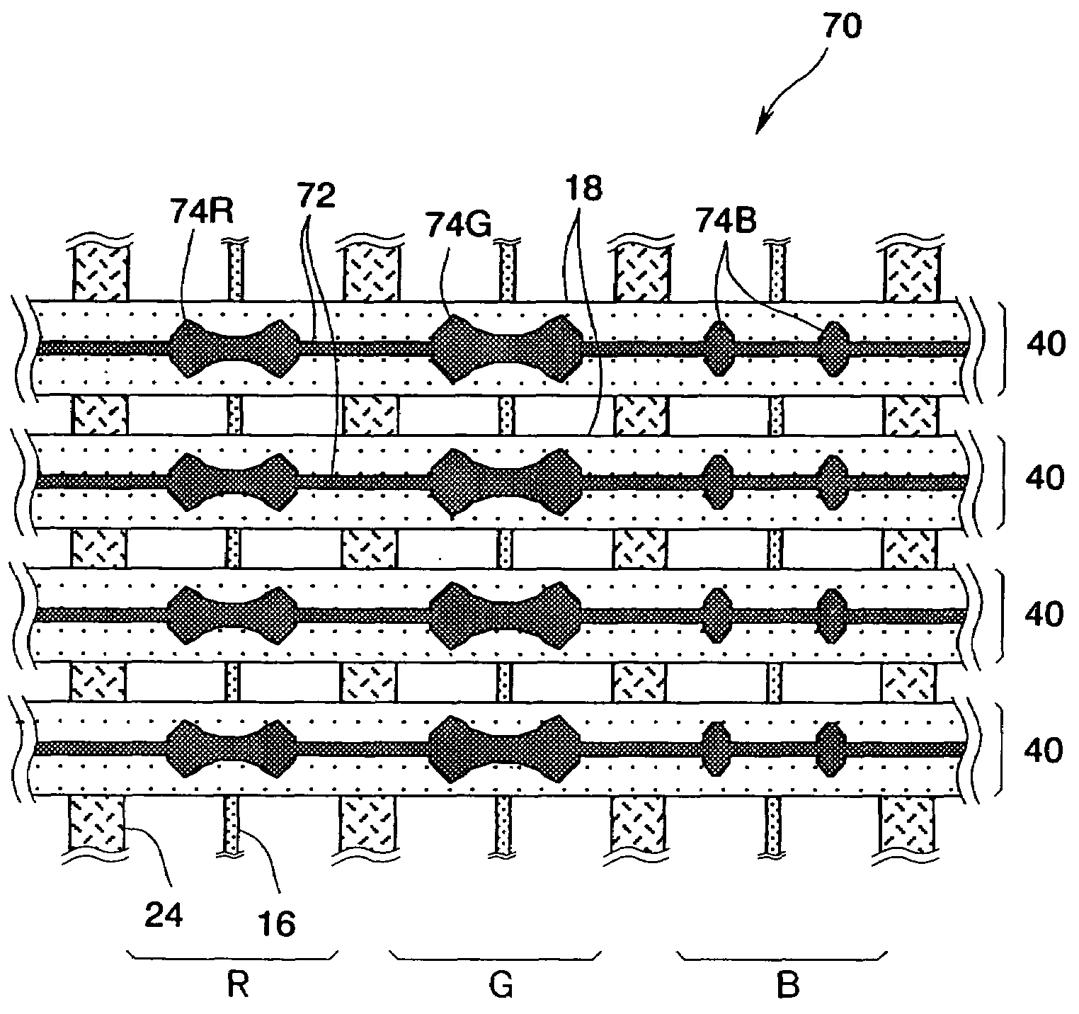
[0080]FIG. 16 shows the essential parts of a seventh embodiment of the plasma display panel in the present invention. The same elements as those described in the conventional art and in the first embodiment will be designated by identical reference numbers. Detailed description thereof will be omitted.

[0081]This embodiment is formed as a PDP 80 of ALIS technology. Shielding parts 82R formed in the cells C that have the phosphor layer R and shielding parts 82G formed in the cells C that have the phosphor layer G are formed in the same shapes and positions as those of the shielding parts 46 in the first embodiment described above while shielding parts 82B formed in the cells C that have the phosphor layer B are formed in conformity with discharging portions. That is, the shielding parts 82B are formed in conformity with portions of higher luminescent brightness. In general, whe...


PUM


Abstract

A plurality of discharge electrodes having transparent electrodes connected to bus electrodes are arranged on the inner side of a front substrate. Alternatively, discharge electrodes having transparent electrodes and capable of discharging between their respective neighboring electrodes on both sides are arranged on the inner side of the front substrate. The front substrate is provided on the side of the display surface where discharge-generated light radiates out to the exterior. Shielding parts for shielding incident light from the exterior are formed on the transparent electrodes, or along the front substrate. Accordingly, the shielding parts reduce the surface reflection to improve the bright room contrast ratio. Forming the shielding parts with the same material as that of the bus electrodes prevents fabrication processes from becoming complicated. The areas of the shielding parts can be varied with the luminescent colors of cells, to change the luminescent brightness by the cell.

Description

BACKGROUND OF THE INVENTION[0001]1. Field of the Invention[0002]The present invention relates to a plasma display panel, and more particularly to a technology for improving a bright room contrast ratio.[0003]2. Description of the Related Art[0004]Plasma display panels (hereinafter, also referred to as PDPs) are display panels of self-luminous type, and are receiving attention as display panels that replace CRTs (Cathode Ray Tubes) by virtue of their high visibility and low profiles. A PDP is formed by filling discharge gas into a space of the order of 100 microns sandwiched between two glass substrates (a front substrate 26 and a rear substrate 34 in FIG. 2 to be described later) which are provided with electrodes. One of the glass substrate is coated with phosphors. Then, a voltage higher than or equal to a starting voltage is applied between the electrodes to cause a discharge, and the ultraviolet rays generated from the discharge make the phosphors excitation-luminous for pixel l...

Claims


Application Information

Patent Timeline
Patent Type & Authority Patents(United States)
IPC IPC(8): H01J17/49H01J11/12H01J11/22H01J11/24H01J11/26H01J11/34H01J11/44
CPCH01J11/12H01J11/24H01J11/44H01J2211/444H01J2211/245
Inventor KANAZAWA, YOSHIKAZUASAO, SHIGEHARU
Owner HITACHI LTD
Why Eureka
Try Eureka