High conducting thin-film nanoprobe card and its fabrication method

a nanoprobe card and high-conductivity technology, applied in nanoinformatics, printed element electric connection formation, instruments, etc., can solve the problems of high frequency and low cost, fabrication cannot meet the demand for ultra-fine pitch, and the future electronic device probing technology will encounter technical challenges

Inactive Publication Date: 2006-03-14
IND TECH RES INST
View PDF7 Cites 135 Cited by
  • Summary
  • Abstract
  • Description
  • Claims
  • Application Information

AI Technical Summary

Benefits of technology

[0008]The present invention has been accomplished under the circumstances in view. It is the main object of the present invention to provide a high conducting thin-film nanoprobe card fabrication met

Problems solved by technology

Future electronic device probing technology will encounter technical challenges in ultra fine pitch, area array testing, high frequency and low cost.
This fabrication cannot satisfy the demand for ultra fine pitch.
1. This kind of probe card does not satisfy technical requirement for 40 GHz probing frequency in RF device testing.
2. Due to the limitation

Method used


Image

  • High conducting thin-film nanoprobe card and its fabrication method
  • High conducting thin-film nanoprobe card and its fabrication method
  • High conducting thin-film nanoprobe card and its fabrication method

Examples


Embodiment Construction

[0028]A high conducting thin-film nanoprobe card fabrication method in accordance with the first embodiment of the present invention includes the steps as follows:

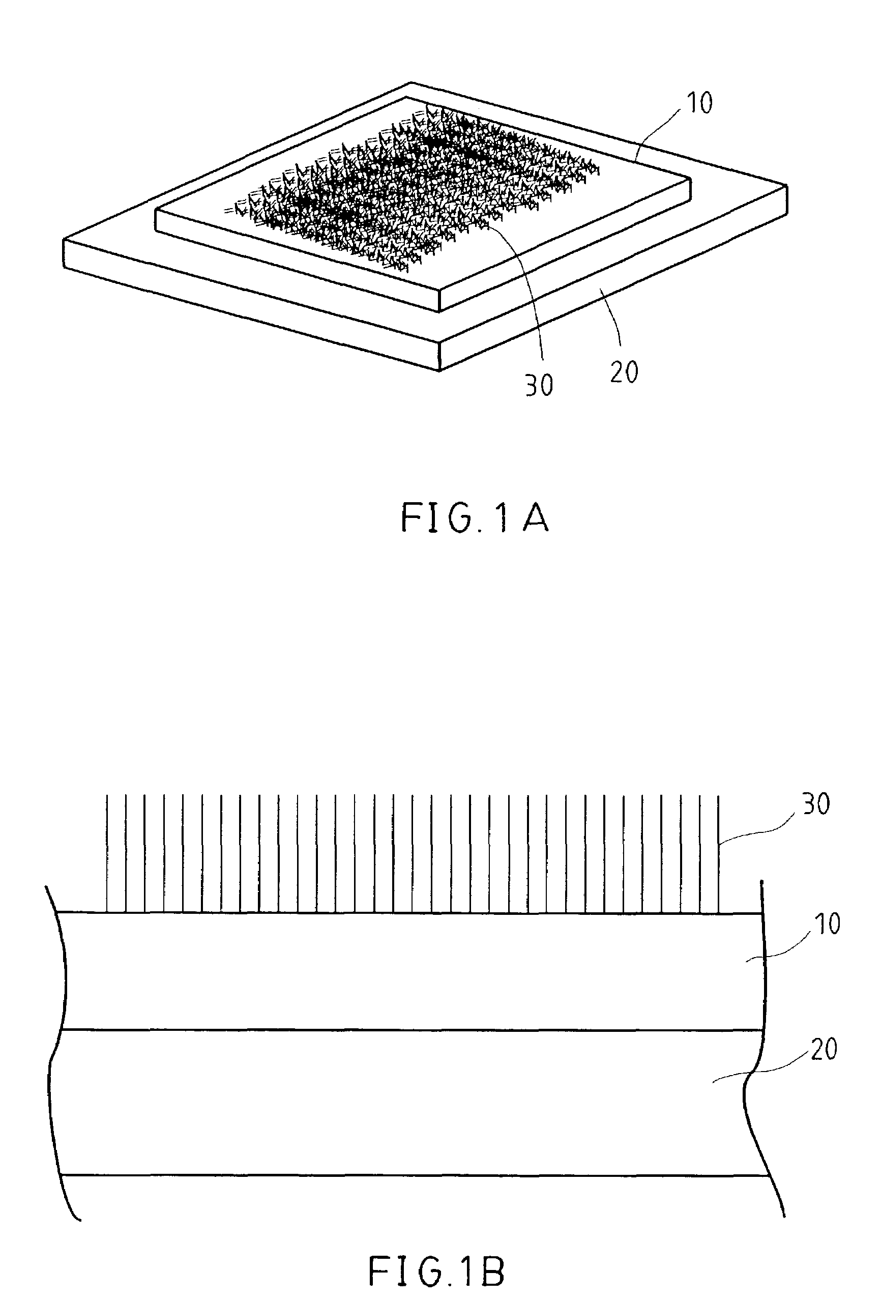
[0029]1. Preparing a substrate 10 of magnetically non-conducting material, then putting the substrate 10 on a flat magnetic plate 20, and then spreading conducting nanotubes or nanowires 30 on the surface of the substrate 10 (see FIG. 1A), and then employing a vacuum evaporating, sputtering, or electroplating technique to coat the nanotubes or nanowires 30 with a layer of magnetically conducting material such as iron or nickel, thereby causing the iron or nickel-coated nanotubes or nanowires 30 to erect from the top side of the substrate 10 due to the effect of the magnetic field of the flat magnetic plate 20 (see FIG. 1B);

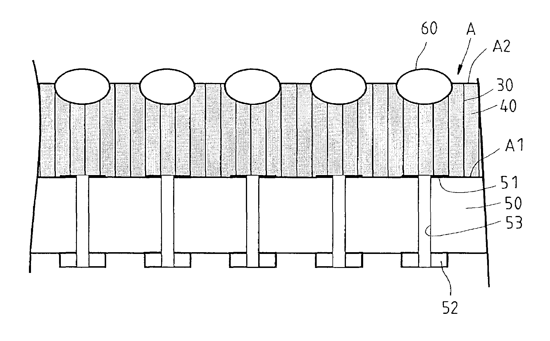
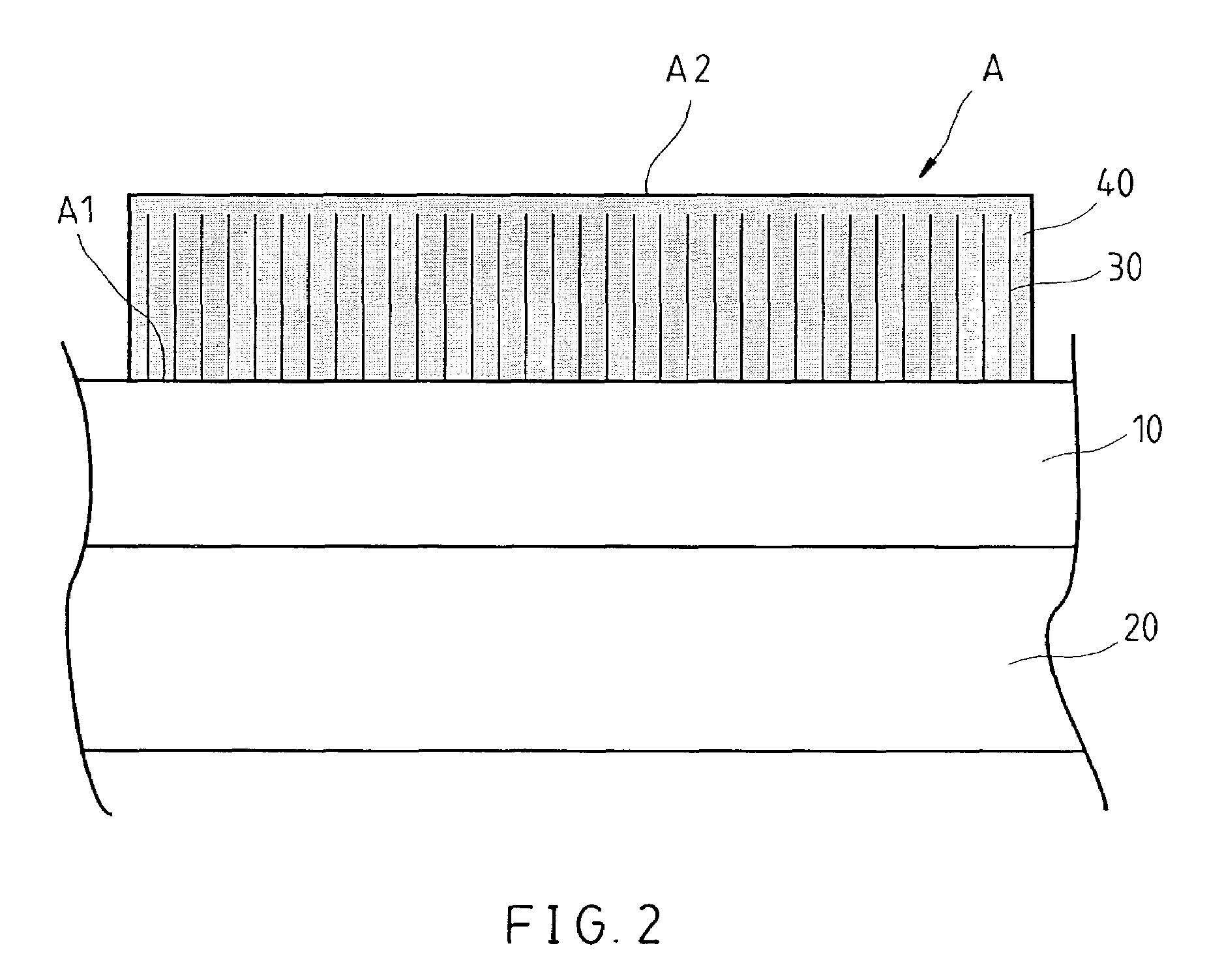
[0030]2. Applying a liquid polymeric resin material 40 of a predetermined viscosity, for example, liquid epoxy resin, polyamide, PMMA, polystyrene or polycarbonate (PC) to the substrate 10 to let the iro...


PUM

PropertyMeasurementUnit
Frequencyaaaaaaaaaa
Electrical conductoraaaaaaaaaa
Deformation enthalpyaaaaaaaaaa

Abstract

A conducting thin-film nanoprobe card fabrication method includes the steps of: (a) arranging nanotubes on a substrate in vertical; (b) covering the nanotubes with a liquid polymeric resin and then hardening the polymeric resin to form a conducting nanomembrane; (c) removing a part of the polymeric resin from the conducting nanomembrane to expose one end of each nanotube to outside; (d) removing the substrate and preparing a ceramic substrate having contacts at one side and metal bumps at the other side and plated through holes electrically respectively connected with the contacts and the metal bumps; (e) mounting the nanomembrane on the ceramic substrate to hold the nanotubes in contact with the contacts of the ceramic substrate, and (f) forming recessed holes in the nanomembrane by etching and inserting a metal rod in each recessed hole to form a respective probe.

Description

BACKGROUND OF THE INVENTION[0001]1. Field of the Invention[0002]The present invention relates generally to the fabrication of probe card for probing electronic devices and, more specifically, to a high conducting thin-film nanoprobe card fabrication method.[0003]2. Description of the Related Art[0004]Future electronic device probing technology will encounter technical challenges in ultra fine pitch, area array testing, high frequency and low cost. Currently, commercialized probing technology for use in high frequency probing includes two types, one is coaxial probe card and ceramic blade probe card, and the other is membrane probe card as disclosed in U.S. Pat. No. 5,090,118. The fabrication of a coaxial probe card or ceramic blade probe card is achieved by mounting coaxial probes or ceramic blade probes in a printed circuit board (PCB) individually. This fabrication cannot satisfy the demand for ultra fine pitch. Further, the maximum probing frequency of a coaxial probe card or cer...

Claims


Application Information

Patent Timeline
IPC IPC(8): G01R31/02G01R1/073G01R3/00H05K3/40
CPCB82Y10/00G01R1/0735G01R3/00Y10T29/49147Y10S977/953Y10T29/49176H05K3/4007
Inventor CHOU, MIN-CHIEHHUANG, YA-JUWANG, HORNG-CHIEH
Owner IND TECH RES INST
Why Eureka
Try Eureka