Quantum optical semiconductor device

a quantum dot and optical semiconductor technology, applied in the field of semiconductor devices, can solve the problems of quantum dot substantial damage, difficult control of steps on such a substrate surface, and extrapolation of conventional processes

Inactive Publication Date: 2006-03-21
FUJITSU LTD
View PDF4 Cites 26 Cited by
  • Summary
  • Abstract
  • Description
  • Claims
  • Application Information

AI Technical Summary

Benefits of technology

[0031]Another and more specific object of the present invention is to provide a quantum semiconductor device having a quantum dot formed by an S-K mode growth process wherein the polarization dependence is eliminated.
[0062]Thus, by forming a quantum optical semiconductor device such that the quantum optical semiconductor device includes therein the quantum dots interacting predominantly with the TM-mode optical radiation in addition to the quantum dots interacting predominantly with the TE-mode optical radiation, or alternatively, by optimizing the strain in each quantum dot such that there occurs interaction to the TM-mode optical radiation in the same proportion with the interaction to the TE-mode optical radiation, it becomes possible to realize an optical semiconductor device free from polarization dependence and thus suitable for use in optical network, and the like.

Problems solved by technology

However, such an approach of extrapolating the conventional process encounters various problems such as difficulty of controlling the steps on such a substrate surface, occurrence of mixing of elements at the quantum-dot interface, and the like.
Further, the use of a patterning process such as lithography for forming the quantum dot inevitably causes substantial damages in the quantum dot.
Thus, it has been difficult to construct a polarization-free device, which is required in the actual optical network systems.
Thus, quantum optical semiconductor devices that use quantum dots formed by the S-K mode growth process generally show remarkable polarization dependence, and because of this, it has been difficult to construct a photonic network, which requires polarization-free optical characteristics for the components constituting the network, by using such conventional quantum optical semiconductor devices unless an additional optical system is provided for compensating for the polarization-dependence of the quantum dots.
However, such an additional optical system is complex and increases the cost of the optical network.

Method used


Image

  • Quantum optical semiconductor device
  • Quantum optical semiconductor device
  • Quantum optical semiconductor device

Examples


first embodiment

[First Embodiment]

[0076]FIG. 3 shows the construction of a quantum optical semiconductor device 10 according to a first embodiment of the present invention.

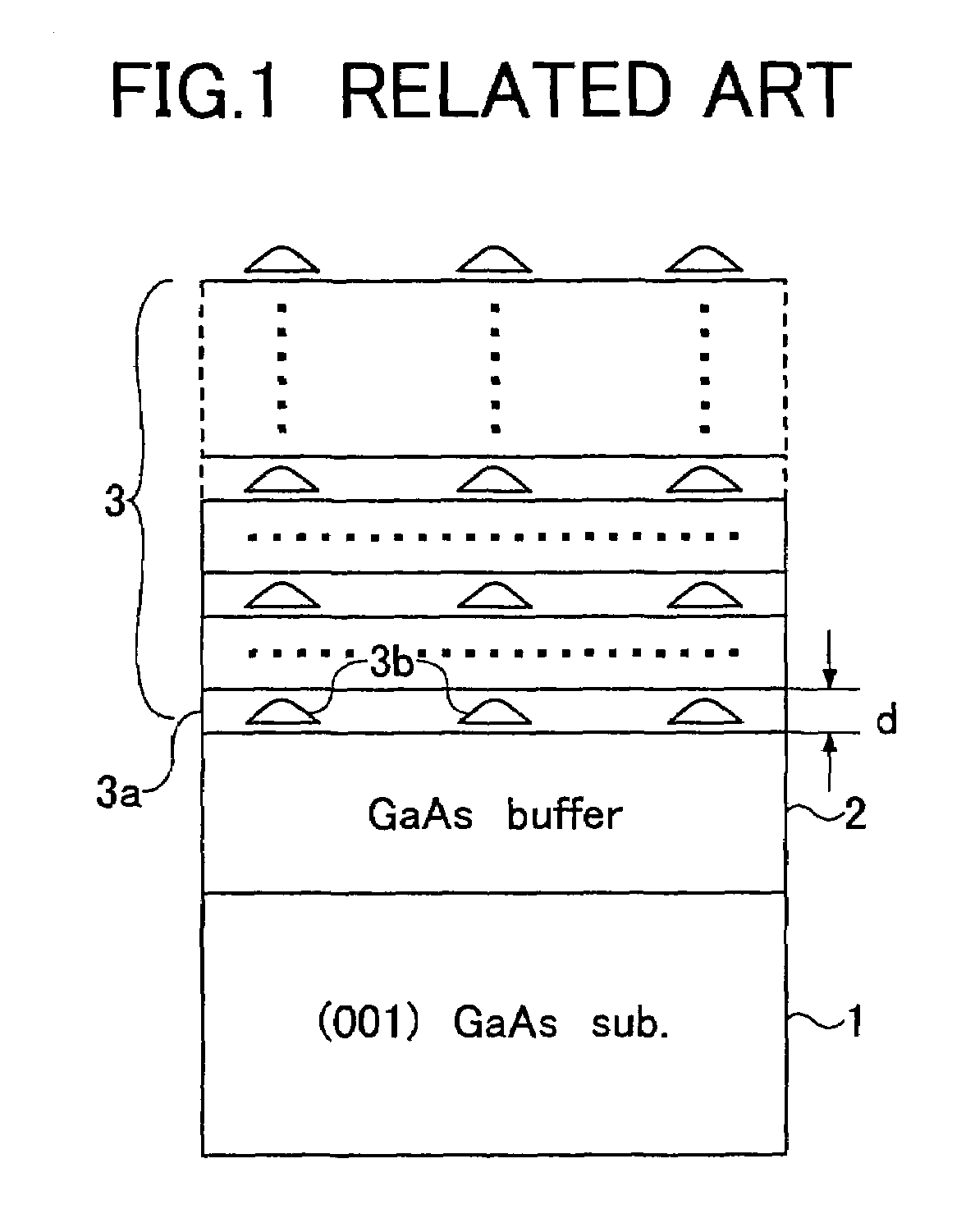
[0077]Referring to FIG. 3, a GaAs buffer layer 12 is formed on a GaAs substrate 11 having a (100)-surface orientation, and an InAs layer is formed on the GaAs buffer layer 12 by an MOVPE process at a substrate temperature of 510° C. with a source supply rate set such that there is formed an InAs layer with a thickness of about 1.8 molecular layers.

[0078]It should be noted that the InAs layer thus formed experiences compressive strain due to the fact that the lattice constant of InAs crystal is larger than the lattice constant of the GaAs substrate, and as a result, there are formed islands of InAs quantum dots 13 on the GaAs buffer layer 12 as a result of the S-K mode growth. Thereby, the InAs quantum dots 13 form a strained heteroepitaxial system together with the underlying GaAs buffer layer 12. It should be noted that such InA...

second embodiment

[Second Embodiment]

[0087]FIG. 5 shows the construction of a quantum optical semiconductor device 20 according to a second embodiment of the present invention.

[0088]Referring to FIG. 5, the quantum optical semiconductor device 20 is constructed on a GaAs substrate of (100)-surface orientation and covered with a buffer layer 22 of GaAs or AlGaAs, wherein the quantum optical semiconductor device 20 further includes a number of InAs quantum dots 23 formed on the buffer layer 22 by an S-K mode growth conducted by using an MOVPE process.

[0089]On the surface on which the S-K growth of the InAs quantum dots 23 occurs, it can be seen that there is formed an extremely thin InAs wetting layer 23a. While not illustrated, a similar wetting layer is used also in the embodiment of FIG. 3.

[0090]In the present embodiment, the InAs quantum dots 23 can be formed by supplying source gases at the substrate temperature of 510° C., for example, with a supply rate set such that there is caused a growth of ...

third embodiment

[Third Embodiment]

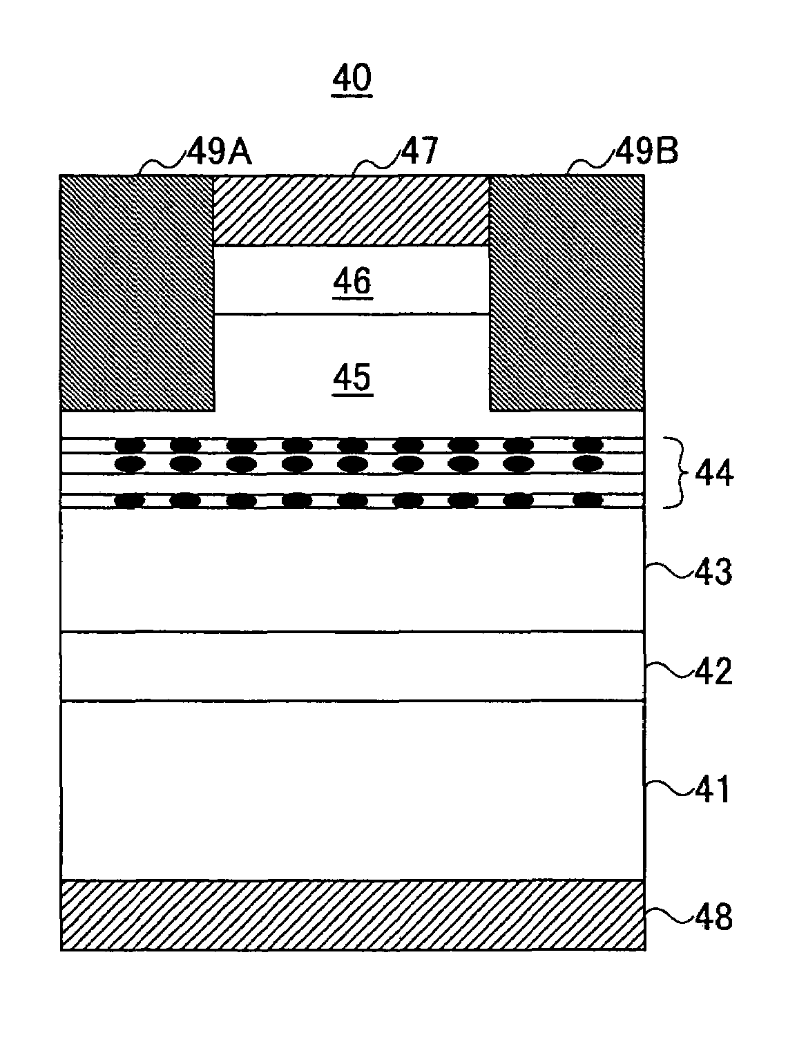
[0098]FIG. 8 shows the construction of a quantum semiconductor device 30 according to a third embodiment of the present invention.

[0099]Referring to FIG. 8, there is formed an InGaAsP barrier layer 32 on an InP substrate 31 having a (100) or (311)B surface orientation via an InP buffer layer not illustrated, and quantum dots 33 of undoped InGaAs or InAs are formed on the InGaAsP barrier layer 32 by an S-K growth process that uses an MOVPE process conducted at the substrate temperature of 450–550° C. As a result of such an S-K growth process, there is formed an extremely thin wetting layer 33A on the surface of the InGaAsP barrier layer 32.

[0100]Further, the quantum dots 33 are buried by another InGaAsP barrier layer 34 having a composition different from the composition of the InGaAsP barrier layer 32, wherein the barrier layer 32 including therein the quantum dots 33 and the barrier layer 34 are deposited alternately and repeatedly for about 10 cycles. Thereby, th...


PUM


Abstract

A quantum semiconductor device including quantum dots formed by S-K growth process taking place in a heteroepitaxial system wherein the relationship between the energy level of light holes and the energy level of heavy holes in the valence band is changed by optimizing the in-plane strain and the vertical strain accumulated in a quantum dot.

Description

CROSS-REFERENCE TO RELATED APPLICATION[0001]The present application is based on Japanese priority application No. 2002-273178 filed on Sep. 19, 2002, the entire contents of which are hereby incorporated by reference.BACKGROUND OF THE INVENTION[0002]1. Field of the Invention[0003]The present invention generally relates to semiconductor devices and more particularly to a quantum optical semiconductor device having a quantum dot structure therein.[0004]2. Description of the Related Art[0005]In a bulk semiconductor crystal where there is no carrier confinement, the state density of the carriers increases continuously with energy in the form of parabolic curve. In a quantum well structure in which there exists one-dimensional carrier confinement, on the other hand, there appear quantum levels as a result of such a one-dimensional carrier confinement, and the state density is changed to have a stepwise form that changes stepwise with energy in correspondence to the quantum levels that cha...

Claims


Application Information

Patent Timeline
Patent Type & Authority Patents(United States)
IPC IPC(8): H01L29/06H01L31/0328H01L31/0336H01L31/072H01L31/109B82Y10/00B82Y20/00B82Y40/00H01L21/205H01L29/12H01L33/00H01L33/06H01L33/30H01S5/343
CPCB82Y10/00B82Y20/00H01L29/127H01L33/06Y10S438/962H01S5/3201H01S5/3412H01S5/5009H01L33/30
Inventor EBE, HIROJINAKATA, YOSHIAKISUGAWARA, MITSURUKITA, TAKASHIWADA, OSAMUARAKAWA, YASUHIKO
Owner FUJITSU LTD
Why Eureka
Try Eureka