Transistor devices, and methods of forming transistor devices and circuit devices

a transistor device and transistor technology, applied in the direction of diodes, capacitors, semiconductor/solid-state device details, etc., can solve the problems of reducing the effective dielectric constant of the dielectric stack, limiting the scalability of the dielectric, and uncontrollable shifts in the threshold voltage of the transistor devi

Inactive Publication Date: 2006-03-28
MICRON TECH INC
View PDF24 Cites 76 Cited by
  • Summary
  • Abstract
  • Description
  • Claims
  • Application Information

AI Technical Summary

Benefits of technology

[0009]The various constructions of the invention can be incorporated into memory devices, such as, for example, DRAM devices. Also, the various constructions of the present invention can be incorporated into electronic systems.

Problems solved by technology

However, such presents several difficulties when utilized in conjunction with the silicon gate electrodes typical of CMOS constructions.
This interfacial layer reduces the effective dielectric constant of the dielectric stack, and thus limits the scalability of the dielectric.
Further, the interfacial layer can be a source of charge trapping / fixed charge, due in part to metal-atom d states and charged atom defects.
The charge trapping / fixed charge can be affected by post-gate annealing, and can result in uncontrollable shifts in a threshold voltage of a transistor device.
Such threshold voltage shifts can be particularly significant and problematic for high thermal budget processing, such as, for example, memory cell processing.
The boron diffusion through the dielectric can be a problem in spite of the thickness increase of the dielectric associated with utilization of a high permittivity film.

Method used


Image

  • Transistor devices, and methods of forming transistor devices and circuit devices
  • Transistor devices, and methods of forming transistor devices and circuit devices
  • Transistor devices, and methods of forming transistor devices and circuit devices

Examples


Embodiment Construction

[0022]This disclosure of the invention is submitted in furtherance of the constitutional purposes of the U.S. Patent Laws “to promote the progress of science and useful arts” (Article 1, Section 8).

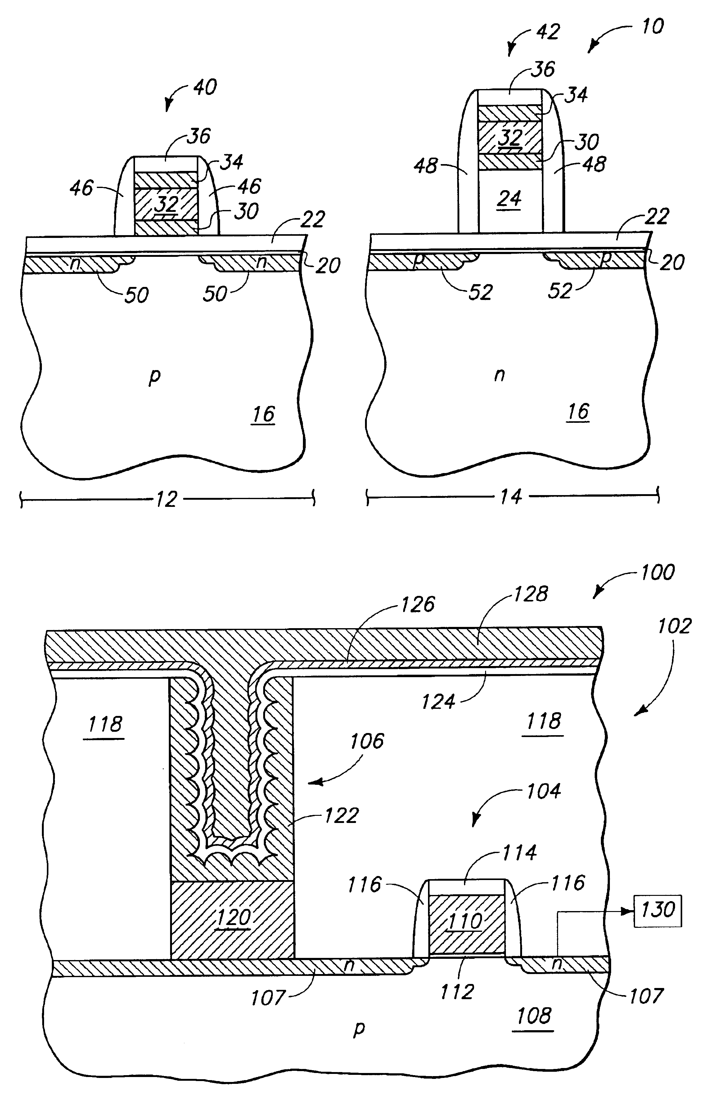
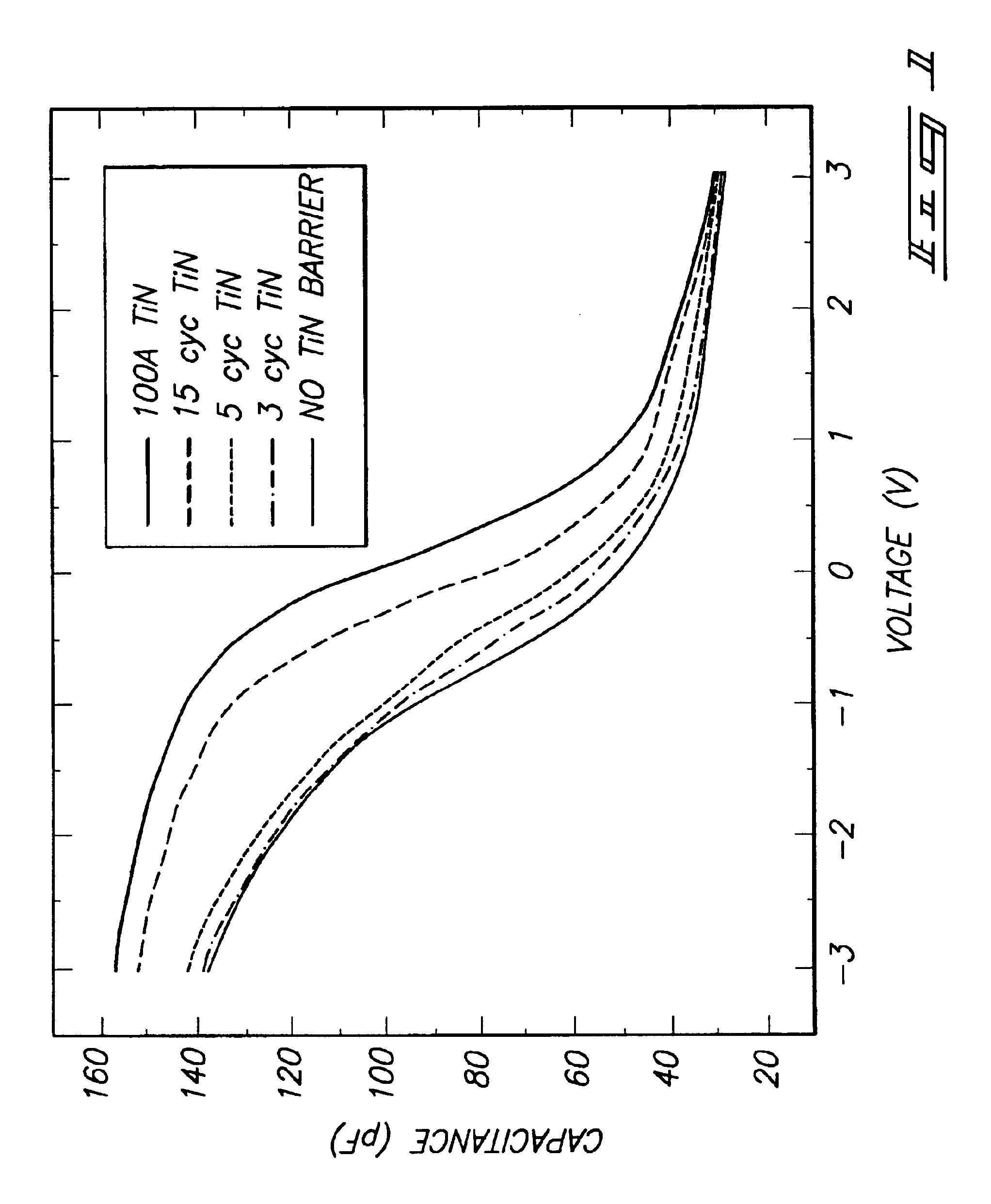
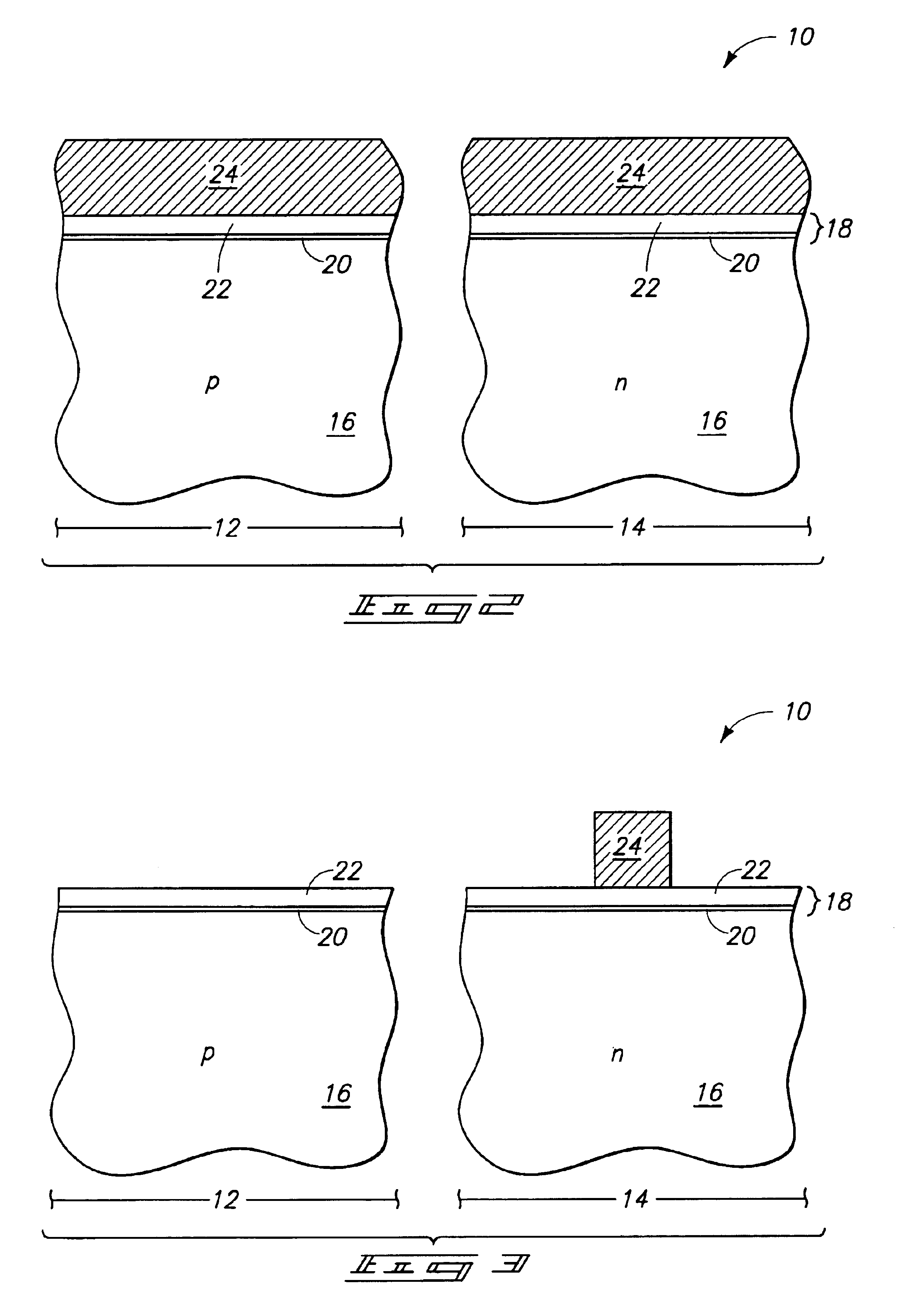
[0023]One aspect of the invention is a recognition that it can be advantageous to incorporate a metal-containing material between dielectric material and conductively-doped silicon in both the NMOS and PMOS devices of CMOS constructions. Further, it is recognized that it can be advantageous if the metal-containing material utilized in the PMOS devices is substantially thicker than the metal-containing material utilized in the NMOS devices (with the metal-containing material in the PMOS devices having a thickness greater than 20 Å, frequently greater than 100 Å, and even greater than or equal to 150 Å), while the metal-containing material utilized in the NMOS devices is thin. The metal-containing material utilized in the NMOS devices is typically no greater than 20 Å, frequently less than ...


PUM

PropertyMeasurementUnit
threshold voltageaaaaaaaaaa
thicknessaaaaaaaaaa
work functionaaaaaaaaaa

Abstract

The invention includes methods of forming circuit devices. A metal-containing material comprising a thickness of no more than 20 Å (or alternatively comprising a thickness resulting from no more than 70 ALD cycles) is formed between conductively-doped silicon and a dielectric layer. The conductively-doped silicon can be n-type silicon and the dielectric layer can be a high-k dielectric material. The metal-containing material can be formed directly on the dielectric layer, and the conductively-doped silicon can be formed directly on the metal-containing material. The circuit device can be a capacitor construction or a transistor construction. If the circuit device is a transistor construction, such can be incorporated into a CMOS assembly. Various devices of the present invention can be incorporated into memory constructions, and can be incorporated into electronic systems.

Description

TECHNICAL FIELD[0001]The invention pertains to transistor devices (including n-channel metal-oxide semiconductor (NMOS) devices and p-channel metal oxide semiconductor (PMOS) devices), and complementary metal-oxide semiconductor (CMOS) constructions. The invention also pertains to methods of making capacitor devices, transistor devices, and CMOS constructions. In particular aspects, the invention pertains to memory storage comprising transistor devices, capacitor constructions and / or CMOS assemblies, and in some aspects the invention pertains to dynamic random access memory (DRAM). In particular aspects, the invention pertains to electronic systems comprising capacitor constructions, transistor devices and / or CMOS assemblies.BACKGROUND OF THE INVENTION[0002]There can be advantages associated with the utilization of high-k gate dielectrics in various semiconductor constructions, including, for example, transistor devices and capacitor devices. High-k dielectrics are understood to be ...

Claims


Application Information

Patent Timeline
Patent Type & Authority Patents(United States)
IPC IPC(8): H01L27/108H01L21/02H01L21/28H01L21/8242H01L27/06H01L29/49H01L29/51
CPCH01L21/28079H01L21/28097H01L21/28194H01L21/28202H01L27/0629H01L27/10808H01L27/10852H01L29/495H01L29/4966H01L29/4975H01L29/513H01L29/517H01L21/28088H01L29/518H01L21/28167H01L28/84H01L28/90H10B12/31H10B12/033H01L21/18H01L21/28H01L29/49
Inventor EPPICH, DENISE M.WEIMER, RONALD A.
Owner MICRON TECH INC
Why Eureka
Try Eureka