Level shift circuit

a level shift and shift circuit technology, applied in logic circuit coupling/interface arrangement, pulse technique, instruments, etc., can solve the problems of insufficient voltage shift amount and operation speed, power consumption increase, and power consumption also low, so as to increase operation speed and voltage shift amount, the effect of increasing the operation speed

Inactive Publication Date: 2006-03-28
LAPIS SEMICON CO LTD
View PDF3 Cites 41 Cited by
  • Summary
  • Abstract
  • Description
  • Claims
  • Application Information

AI Technical Summary

Benefits of technology

[0012]According to the present invention, the fifth transistor circuit is installed, so the ratio of the inflow current and the emission current of the first node or the second node can be switched according to the control signal. By this, the operation speed can be increased by setting this ratio to high, an

Problems solved by technology

However, even with the level shift circuit in FIG. 12B, a sufficient voltage shift amount and operation speed cannot be obtained.
If the current capability of these MOS transistors 1211–1214 is too high, however, the through current generated when both MOS transistors 1211 and 1213 turn ON or when both MOS transistors 1212 and 1214 turn ON becomes extremely high, so power consumption increases, which is another problem.
As a result, the level shift circuit can accurately operate at high-speed, and power consumption is also low.
Power consumption, however, is high, since the through current increases when the control signal L-SPEED is set to high level.
As a result, the level shift circuit can accurately operate at high-speed, and power consumption is also low.
Power consumption, however, is high since the through current increases.
Power consumption, however, is high, since the through current increases when the control signal L-SPEED is set to high level.
As a result, the level shift circuit can accurately operate at high-speed, and power consumption is also low.
However, the level shift circuit can be operated normally

Method used


Image

  • Level shift circuit
  • Level shift circuit
  • Level shift circuit

Examples


first embodiment

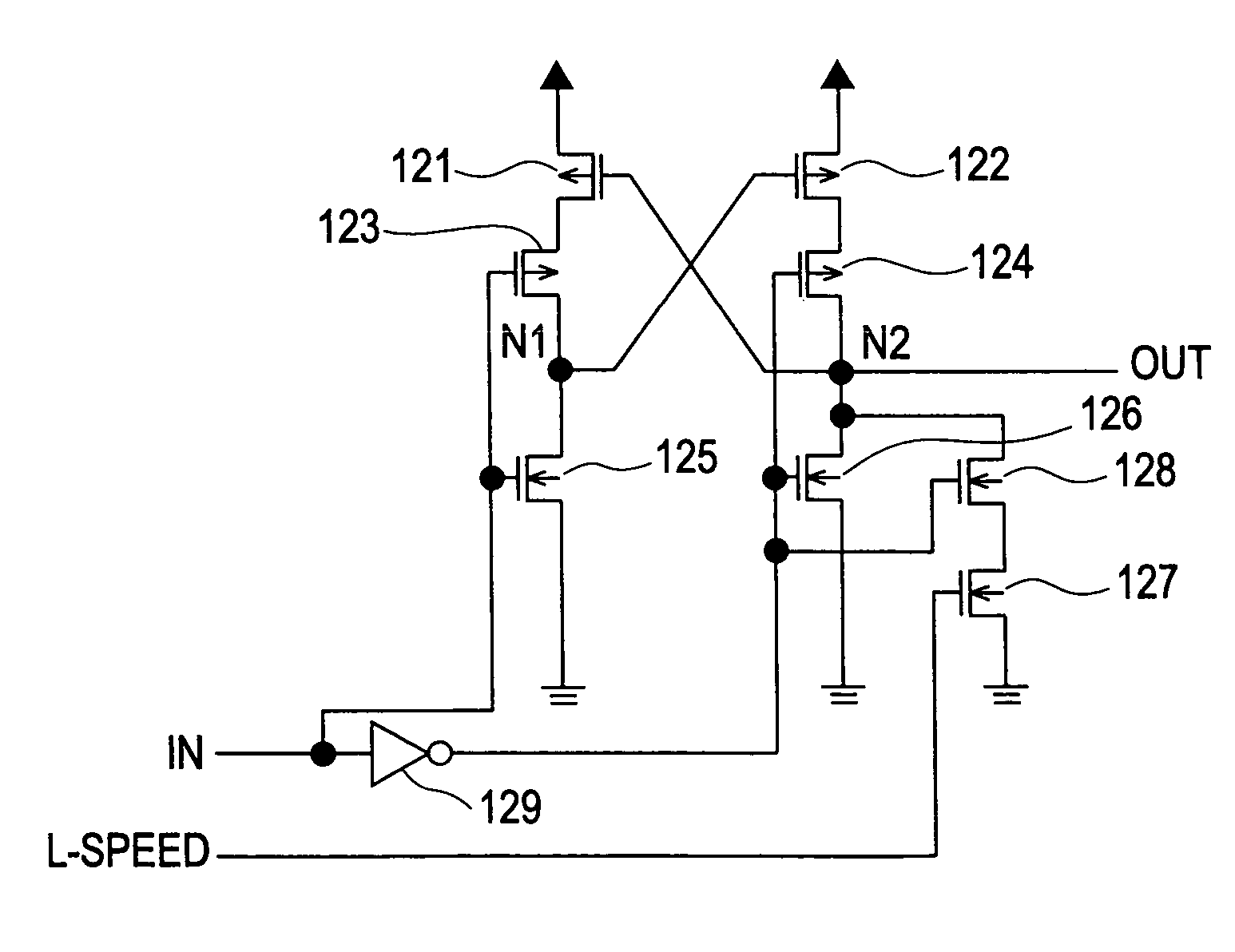
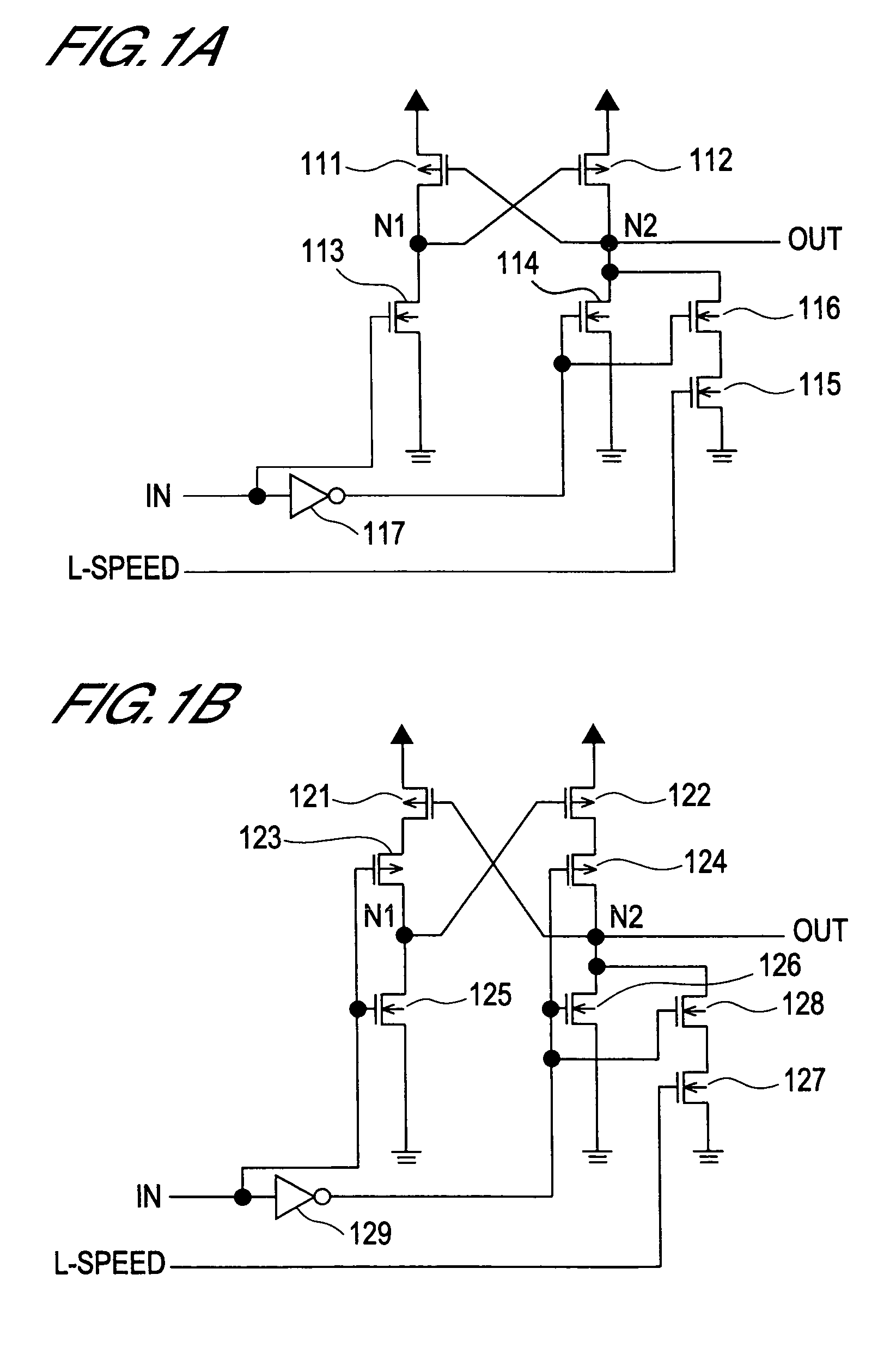
[0047]FIG. 1A is a circuit diagram depicting the configuration of key components of the level shift circuit according to the present embodiment. As shown in FIG. 1A, this level shift circuit is comprised of the pMOS transistors 111 and 112, the nMOS transistors 113, 114, 115 and 116, and the inverter 117.

[0048]In the pMOS transistor 111, the source is connected to the power supply line (not illustrated), the drain is connected to the node N1, and the gate is connected to the node N2.

[0049]In the pMOS transistor 112, the source is connected to the power supply line, the drain is connected to the node N2, and the gate is connected to the node N1. Here, in order to recharge the node N2 at high-speed, it is preferable that the current capability of the pMOS transistor 112 is sufficiently high.

[0050]In the nMOS transistor 113, the source is connected to the ground line (not illustrated), the drain is connected to the node N1, and the input signal IN is input from the gate.

[0051]In the nM...

second embodiment

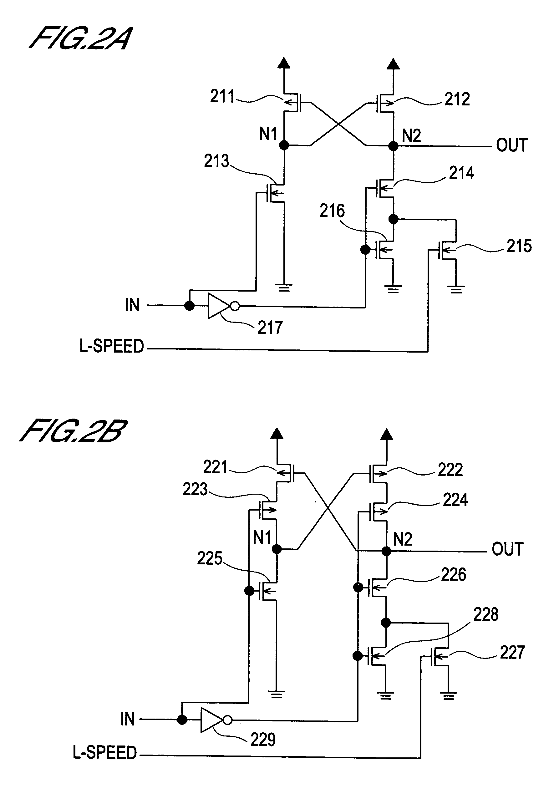
[0089]FIG. 2A is a circuit diagram depicting the configuration of key components of the level shift circuit according to the present embodiment. As shown in FIG. 2A, this level shift circuit is comprised of the pMOS transistors 211 and 212, the nMOS transistors 213–216, and the inverter 217.

[0090]In the pMOS transistor 211, the source is connected to the power supply line, the drain is connected to the node N1, and the gate is connected to the node N2.

[0091]In the pMOS transistor 212, the source is connected to the power supply line, the drain is connected to the node N2, and the gate is connected to the node N1. In order to recharge the node N2 at high-speed, it is preferable that the current capability of the pMOS transistor 212 is sufficiently high.

[0092]In the nMOS transistor 213, the source is connected to the ground line, the drain is connected to the node N1, and the input signal IN is input from the gate.

[0093]In the nMOS transistor 214, the drain is connected to the node N2...

third embodiment

[0131]FIG. 3A is a circuit diagram depicting the configuration of key components of the level shift circuit according to the present embodiment. As shown in FIG. 3A, this level shift circuit is comprised of the pMOS transistors 311 and 312, the nMOS transistors 313–318, and the inverter 319.

[0132]In the pMOS transistor 311, the source is connected to the power supply line, the drain is connected to the node N1, and the gate is connected to the node N2. In order to recharge the node N1 at high-speed, it is preferable that the current capability of the pMOS transistor 311 is sufficiently high.

[0133]In the pMOS transistor 312, the source is connected to the power supply line, the drain is connected to the node N2, and the gate is connected to the node N1. In order to recharge the node N2 at high-speed, it is preferable that the current capability of the pMOS transistor 312 is sufficiently high.

[0134]In the nMOS transistor 313, the source is connected to the ground line, the drain is co...


PUM


Abstract

A level shift circuit including a first transistor circuit connected between a power supply line and a first node, a second transistor circuit connected between the power supply line and a second node, a first transistor connected between the ground line and the first node, and a second transistor connected between the ground line and the second node. A gate of the first transistor circuit is connected to the second node, and a gate of the second transistor circuit is connected to the first node. An input signal is supplied to a gate of the first transistor and an inverted value of the input signal is supplied to a gate of the second transistor. Additionally, control transistors switch a ratio of inflow current and emission current of the first node or the second node according to a control signal.

Description

CROSS REFERENCE TO RELATED APPLICATIONS[0001]This is a divisional application of application Ser. No. 10 / 073,022, filed Feb. 12, 2002 is now abandoned, which is hereby incorporated by reference in its entirety for all purposes.BACKGROUND OF THE INVENTION[0002]1. Field of the Invention[0003]The present invention relates to a level shift circuit used for a semiconductor integrated circuit for example, and more particularly to a technology to increase the speed of operation of the level shift circuit.[0004]2. Description of Related Art[0005]In some cases a plurality of types of circuits are installed on one electronic equipment or on one circuit board. In such a case, signals are transmitted / received between each circuit. In the case of digital signals, two types of values, that is, low level or high level, are transmitted / received. The value of low level is often zero volts. And the value of high level is for example 1.5 volts, 3 volts and 5 volts. In some cases circuits with differen...

Claims


Application Information

Patent Timeline
IPC IPC(8): H03K19/0175G05F3/24H03K3/012H03K19/00H03K3/356H03K17/16H03K19/0185
CPCH03K3/012H03K3/356113H03K17/164
Inventor KOUZUMA, SHINICHI
Owner LAPIS SEMICON CO LTD
Why Eureka
Try Eureka