Reduced cross-contamination between chambers in a semiconductor processing tool

a technology of cross-contamination and processing tools, applied in the direction of lighting and heating apparatus, charge manipulation, furnaces, etc., can solve the problems of contaminating the other chamber and the inability to ensure the pressure differential between the chambers

Active Publication Date: 2006-04-04
ASM IP HLDG BV
View PDF29 Cites 15 Cited by
  • Summary
  • Abstract
  • Description
  • Claims
  • Application Information

AI Technical Summary

Benefits of technology

[0007]The present method ensures the occurrence of the desired flow between the transfer chamber and the process chamber(s) upon opening of the gate valve(s) between the chambers.

Problems solved by technology

Gaseous (homogeneous) cross-contamination takes place when gases from one chamber are convectively or diffusively transported to another chamber, thereby contaminating the other chamber.
One problem with such systems is that creating a pressure differential between the chambers does not necessarily ensure that the desired gas flow will occur upon opening of the gate valve.

Method used


Image

  • Reduced cross-contamination between chambers in a semiconductor processing tool
  • Reduced cross-contamination between chambers in a semiconductor processing tool
  • Reduced cross-contamination between chambers in a semiconductor processing tool

Examples


Embodiment Construction

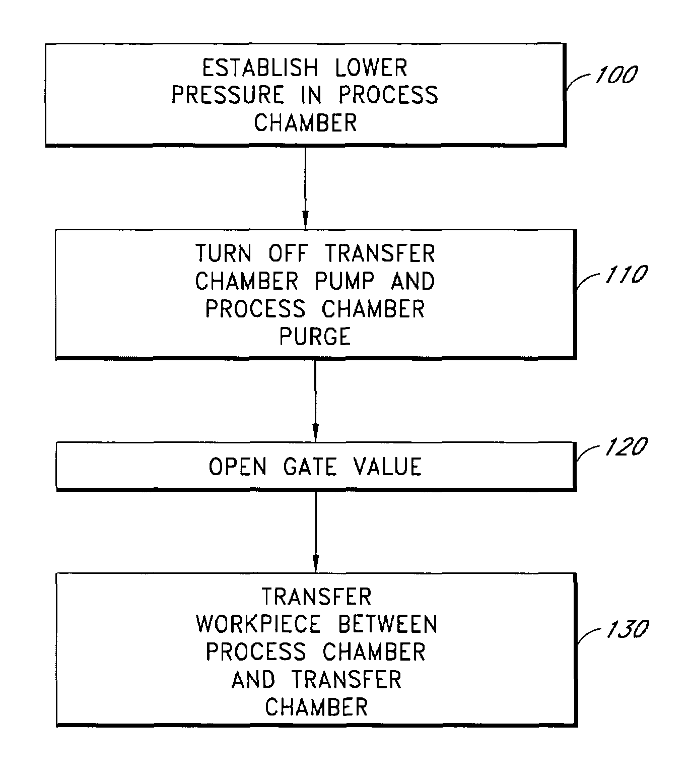
[0017]While not separately illustrated in the figures, it will be understood that the process steps disclosed herein can be programmed into a process tool controller that is electrically connected to control gas flow valves, mass flow controllers, gate valve actuators, substrate transfer robots, etc. The skilled artisan will readily appreciate that an apparatus can be provided with software programming or hard wiring to achieve the desired processing steps described herein.

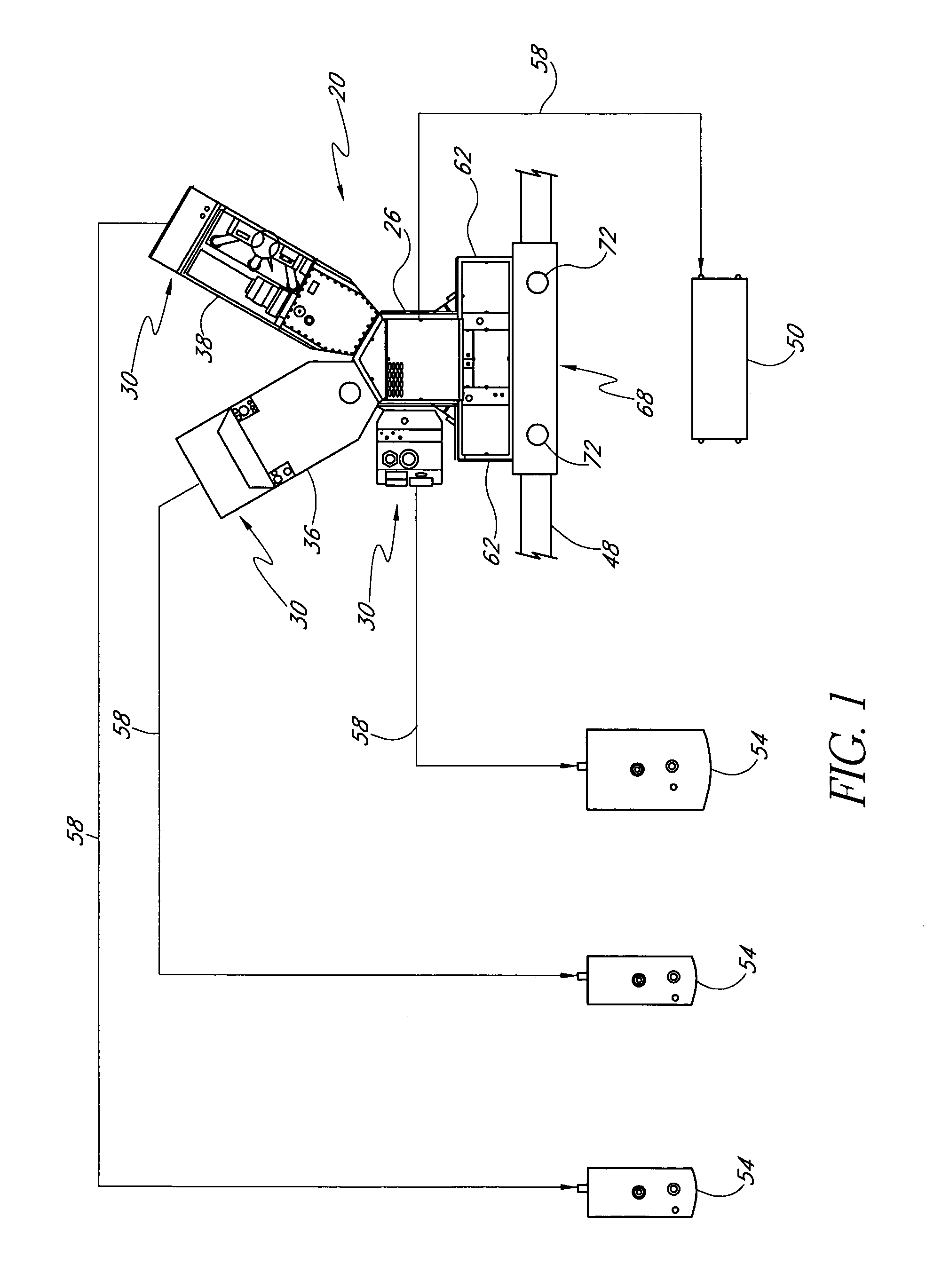
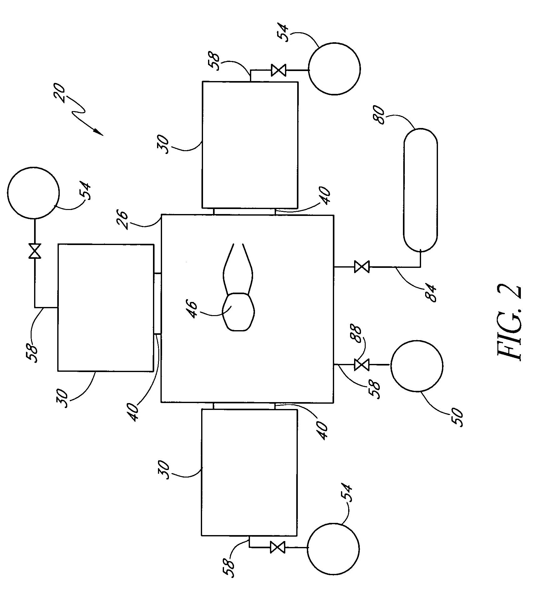
[0018]With reference initially to FIG. 1, an exemplary semiconductor processing apparatus 20 is illustrated, comprising a central substrate or workpiece handling chamber, or referred to herein as a transfer chamber 26, connected to at least one process chamber. FIG. 1 shows the handling chamber 26 surrounded by a number of process chambers 30. In the illustrated embodiment, the semiconductor processing apparatus 20 is adapted for use in CMOS gate stack applications. The process chambers 30 comprise a hydrogen fluo...


PUM

PropertyMeasurementUnit
pressureaaaaaaaaaa
pressureaaaaaaaaaa
pressureaaaaaaaaaa

Abstract

In accordance with one aspect of the present invention, a method is provided for transporting a workpiece in a semiconductor processing apparatus comprising a transfer chamber, a process chamber, and a gate valve between the transfer chamber and the process chamber. The method comprises vacuum pumping the transfer chamber to achieve a first pressure in the transfer chamber and vacuum pumping the process chamber to achieve a second pressure in the process chamber. An inert gas is flowed into the transfer chamber and shut off in the process chamber. The transfer chamber is isolated from pumping, but pumping continues from the process chamber. The gate valve is opened after isolating the transfer chamber from pumping. The workpiece is then transferred between the transfer chamber and the process chamber. A definitive flow direction from transfer chamber to process chamber is thereby achieved, minimizing risk of back-diffusion.

Description

REFERENCE TO RELATED APPLICATION[0001]This application is a continuation of U.S. Ser. No. 10 / 441,642, filed May 20, 2003, issued Sep. 28, 2004 as U.S. Pat. No. 6,797,617, and claims priority benefit under 35 U.S.C § 119(e) to U.S. provisional application No. 60 / 382,204, filed May 21, 2002.FIELD OF THE INVENTION[0002]The present invention relates to semiconductor processing tools and, in particular, to methods of minimizing cross-contamination during transport of the wafers between chambers of such tools.BACKGROUND OF THE INVENTION[0003]Cluster tools used in the semiconductor processing of wafers or other workpieces typically comprise a central wafer handling chamber, or transfer chamber, surrounded by a number of process chambers within which various processes are carried out on the wafers (e.g., deposition, etching, doping, annealing and oxidizing). A robot is provided in the transfer chamber for moving the wafers within the cluster tool. The transfer chamber is typically isolated ...

Claims


Application Information

Patent Timeline
Patent Type & Authority Patents(United States)
IPC IPC(8): H01L21/302B65G49/00H01L21/00H01L21/205H01L21/3065H01L21/677
CPCH01L21/67017H01L21/67748Y10S438/908H01L21/00H01L21/02
Inventor POMAREDE, CHRISTOPHESHERO, ERIC J.JYLHA, OLLI
Owner ASM IP HLDG BV
Why Eureka
Try Eureka