Liquid crystal display panel, liquid crystal display device, and liquid crystal television

Inactive Publication Date: 2006-04-11
PANASONIC LIQUID CRYSTAL DISPLAY CO LTD +1
View PDF7 Cites 29 Cited by
  • Summary
  • Abstract
  • Description
  • Claims
  • Application Information

AI Technical Summary

Benefits of technology

[0013]An object of the present invention is to provide a liquid crystal display panel

Problems solved by technology

In such a system, a tone of color can be inverted depending on the direction in which the viewer watches the screen of a liquid crystal panel, particularly in the case of a halftone, presenting a big problem of allowing only a narrow viewing angle range.
The biggest problem with the existing IPS liquid crystal display device is to determine how the response speed can be increased, considering its future applications in display devices supporting moving pictures, such as liquid crystal televisions and DVD video reproducing monitors.
This tradeoff relationship, coupled with the fact that the characteristics of a liquid crystal material directly affect the display characteristics of, as well as the reliability in, the liquid crystal display device, imposes restrictions on the latitude allowed in material development; and, thus, there is a limit to achievement of a higher speed response merely from the approach of material development.
Overdrive driving is a means effective only in the case of a halftone, and the biggest problem with this method is that it is unable to improve the response speed throughout all gradations.
This means that the method is unable to increase the response speed, with which gradations are rendered by the no voltage condition.
Moreover, on the high voltage side, too, the voltage to be applied to the pixel is limited because of the electrical withstand voltage of the signal line driver, and it is generally equivalent to one that sufficiently drives the liquid crystal (operat

Method used


Image

  • Liquid crystal display panel, liquid crystal display device, and liquid crystal television
  • Liquid crystal display panel, liquid crystal display device, and liquid crystal television
  • Liquid crystal display panel, liquid crystal display device, and liquid crystal television

Examples


embodiment 1

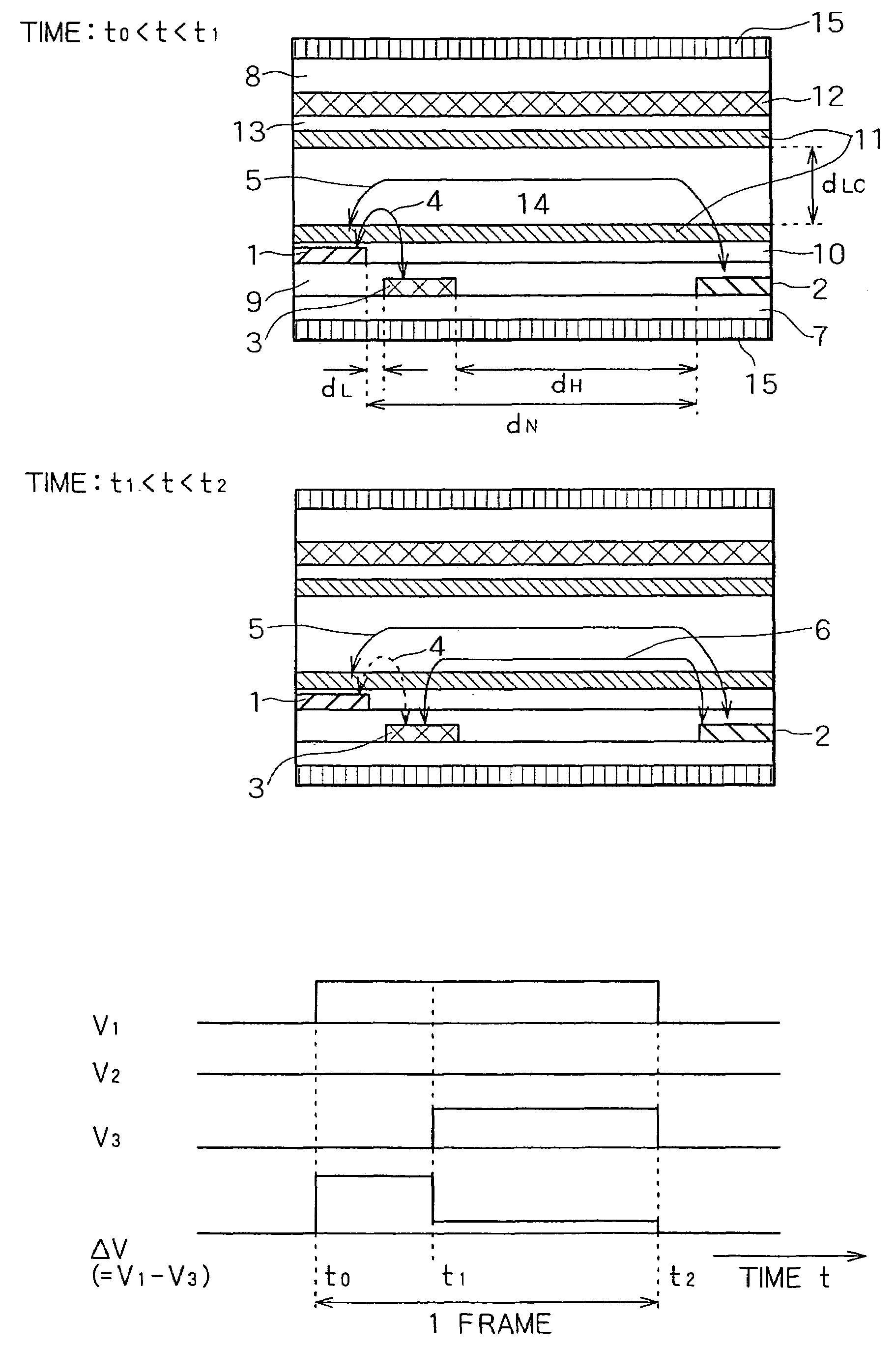
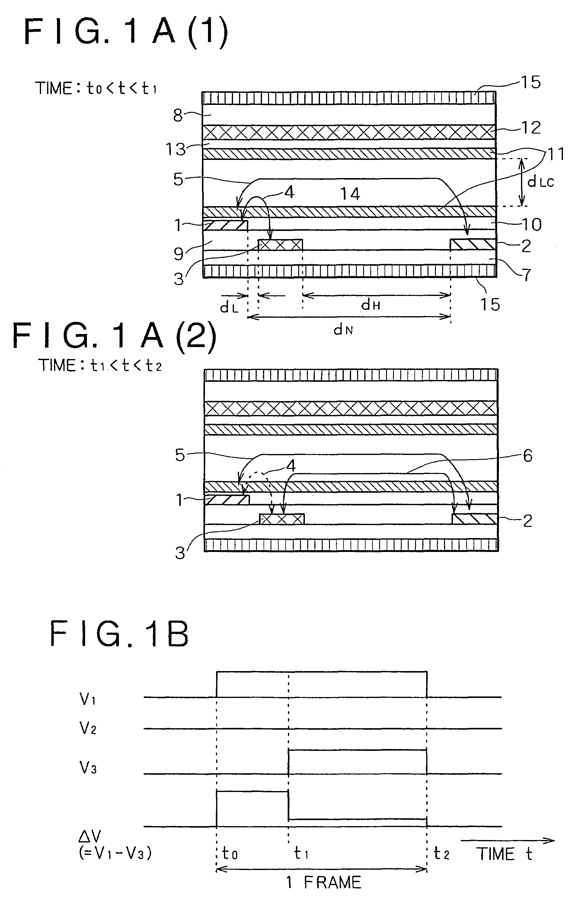
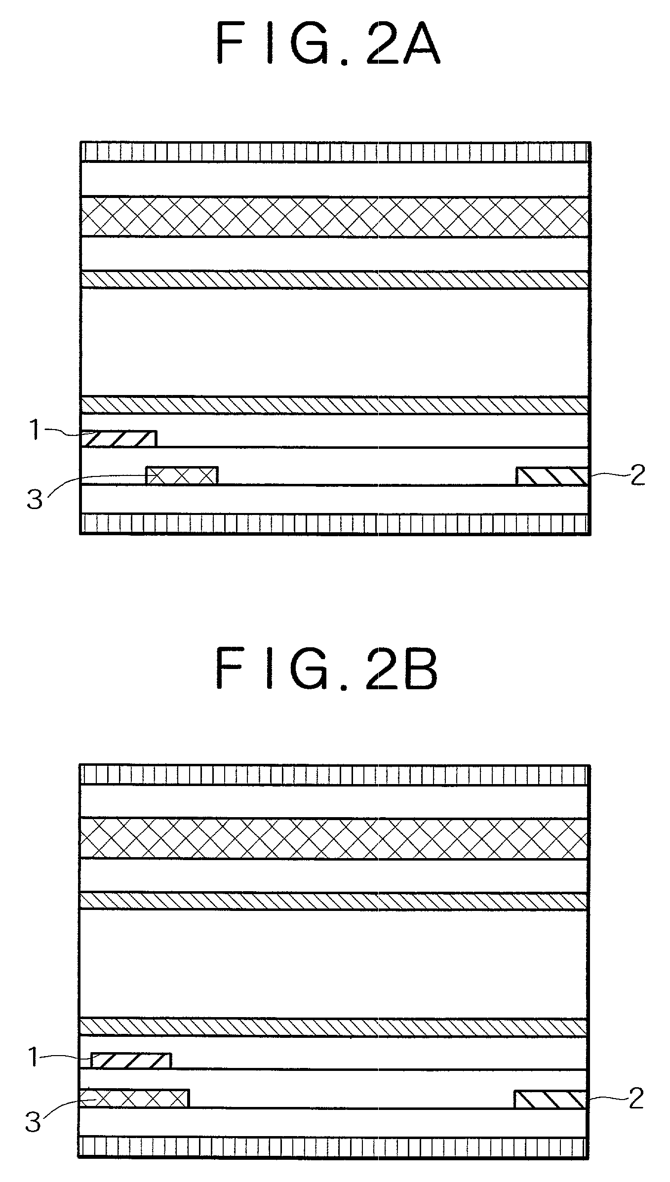
[0090]The arrangement according to Embodiment 1 will be explained with reference to FIGS. 3, 4, 5, 6, 7A and 7B. FIG. 3 illustrates the electrode structure of a pixel portion in a liquid crystal display panel according to Embodiment 1. FIG. 4 is a cross-sectional view showing the pixel portion in the liquid crystal display panel according to Embodiment 1. FIG. 5 shows the signal waveforms of signals supplied to the different electrodes and lines shown in FIG. 3. FIG. 6 is a schematic diagram showing the overall structure of the liquid crystal display device having these pixel structures. For the purpose of this specification, the term “liquid crystal display panel” is used to refer to a device which includes a pair of substrates, a liquid crystal layer, electrodes disposed on the pair of substrates, and the like, as shown in FIGS. 1 and 4, and the term “liquid crystal display device” is used to refer to a system combining the liquid crystal display panel, a light source, and the lik...

embodiment 2

[0113]The arrangement of a second embodiment according to the present invention will be explained with reference to FIGS. 10 and 11. FIG. 10 includes diagrams of the electrode structure of a pixel portion. FIG. 11 shows the signal waveforms supplied to different electrodes and lines disposed as shown in FIG. 10.

[0114]The arrangement of a liquid crystal display panel according to Embodiment 2 differs from that of the liquid crystal display device according to Embodiment 1 in that a third electrode 107 and a pixel electrode 106 are superposed on each other. Because of this configuration, the pixel electrode 106 must be disposed on a layer above the layer on which a first signal line 104 is disposed; and, as shown in FIG. 10B, the pixel electrode 106 is disposed on an even higher layer by way of a through-hole 113, being superposed on the third electrode 107. Since the third electrode 107 is superposed on the pixel electrode 106, signal waveforms supplied to different electrodes and li...

embodiment 3

[0122]The arrangement of a third embodiment according to the present invention will be explained with reference to FIGS. 13, 14, and 15. FIG. 13 shows a view of the electrode structure of a pixel portion. FIG. 14 shows signal waveforms supplied to different electrodes and lines. FIG. 15 is a schematic diagram showing the overall structure of the liquid crystal display panel having these pixel structures.

[0123]The arrangement of the liquid crystal display panel according to Embodiment 3 differs from that of the liquid crystal display device according to Embodiment 1 in that two TFTs disposed within one pixel are driven by one scanning line. The reduction in the number of scanning lines by one from the arrangement according to Embodiment 1 yields the effect that a second scanning line driver is no longer necessary.

[0124]As shown in FIG. 13, the electrode structure according to Embodiment 3 is provided with two TFTs, one scanning line, and two signal lines in order to drive one pixel. ...


PUM


Abstract

To provide a high-quality liquid crystal display device that does not produce image sticking and that can realize high response speed, a third electrode is provided that is different from a common electrode or a pixel electrode, and a voltage applied to the third electrode is varied within one frame period to drive a liquid crystal using a strong electric field and a uniform horizontal electric field in an initial stage within one frame period, while driving the liquid crystal only with the uniform horizontal electric field in a latter stage within one frame period.

Description

BACKGROUND OF THE INVENTION[0001]The present invention relates to an active matrix type liquid crystal display panel, an active matrix type liquid crystal display device, and a liquid crystal television.[0002]A liquid crystal display device is composed essentially of two glass substrates that are separated to form a predetermined space into which a layer of liquid crystal is injected. A polymer thin film, called an alignment film, is disposed between the glass substrate and the liquid crystal layer, and the alignment film is processed for aligning the liquid crystal molecules. Displays are produced by such liquid crystal display devices as follows. That is, when an electric field is applied to the orderly arrangement of liquid crystal molecules, it changes the alignment direction of the molecules, which, in turn, results in a change in the optical characteristics in the liquid crystal layer.[0003]In the conventional active drive type liquid crystal display device, a transparent elec...

Claims


Application Information

Patent Timeline
IPC IPC(8): G09G3/36G02F1/13G02F1/133G02F1/1343G02F1/1345G02F1/1368G09F9/30G09F9/35G09G3/20G09G3/34H04N5/66
CPCG02F1/134363G09G3/3659G09G2300/043G09G2320/0257G09G2320/02G09G2320/0252G09G2300/0809G02F1/133
Inventor OKISHIRO, KENJIOAKU, HITOSHIHIYAMA, IKUOKONDOU, KATSUMI
Owner PANASONIC LIQUID CRYSTAL DISPLAY CO LTD
Why Eureka
Try Eureka