Patterned substrate and liquid crystal display provided therewith

a liquid crystal display and substrate technology, applied in the field of patterned substrates and liquid crystal displays, can solve the problems of reducing yield, unable to partially form al metal films, and above-described conventional liquid crystal displays

Inactive Publication Date: 2006-04-18
SHARP KK
View PDF9 Cites 29 Cited by
  • Summary
  • Abstract
  • Description
  • Claims
  • Application Information

AI Technical Summary

Benefits of technology

[0026]According to the above constitution, an Al metal film is used as the reflective metal film and an indium-tin oxide (ITO) film functioning as terminals for connecting with a driver and a transparent electrode is formed on the substrate. Even in the case of patterning the Al metal film formed on the ITO film, electrolytic corrosion between the Al metal film and the ITO film is prevented since the Mo film is formed between the Al metal film and the ITO film.

Problems solved by technology

The above-described conventional liquid crystal display, however, has problems as described below.
That is, when a reflective electrode is formed by forming an Al metal film on a resin film having a plurality of concave and convex portions formed thereon as described above, it is impossible to partially form an Al metal film, particularly in a mass production process, unless a special film forming method such as mask-deposition or the like is used.
However, the following problem is caused when this reflective electrode film (Al metal film) is patterned.
As a result, the Al film and the ITO film are corroded and melted and thereby the yield decreases.
By the way, in the case of patterning a metal film such as Al or the like formed on the resin film as a reflective electrode or a transparent conductive film, the metal film often peels because the adhesion between the resin film and the metal film is weakened due to the swelling of the resin film by a resist remover.
In general, in the case where metal wiring is provided on an insulator such as a polymeric film or the like, the problem is that the adhesion between the polymeric film and the metal film is weak.
However, there is a problem that sufficient adhesion cannot be obtained even by sputtering when the aforementioned Mo film is formed.

Method used


Image

  • Patterned substrate and liquid crystal display provided therewith
  • Patterned substrate and liquid crystal display provided therewith
  • Patterned substrate and liquid crystal display provided therewith

Examples


first embodiment

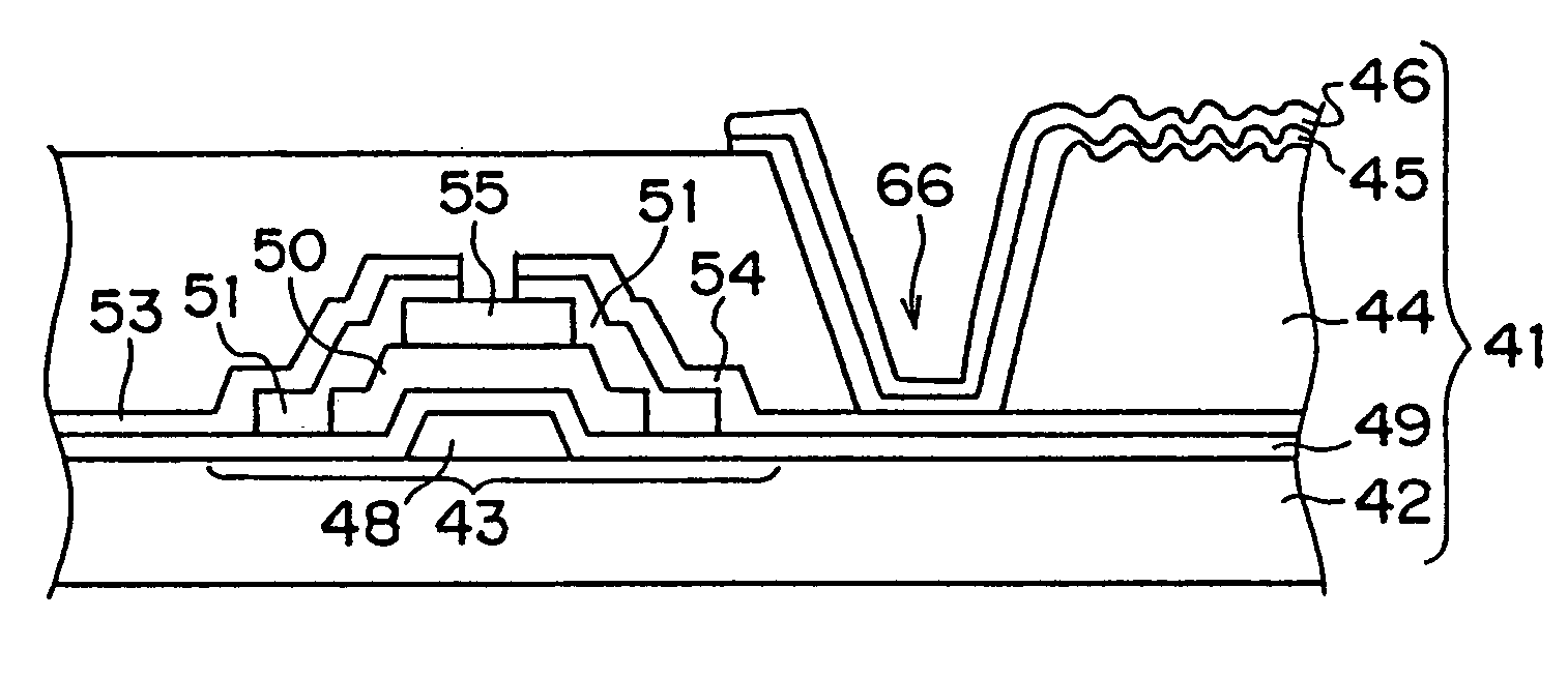
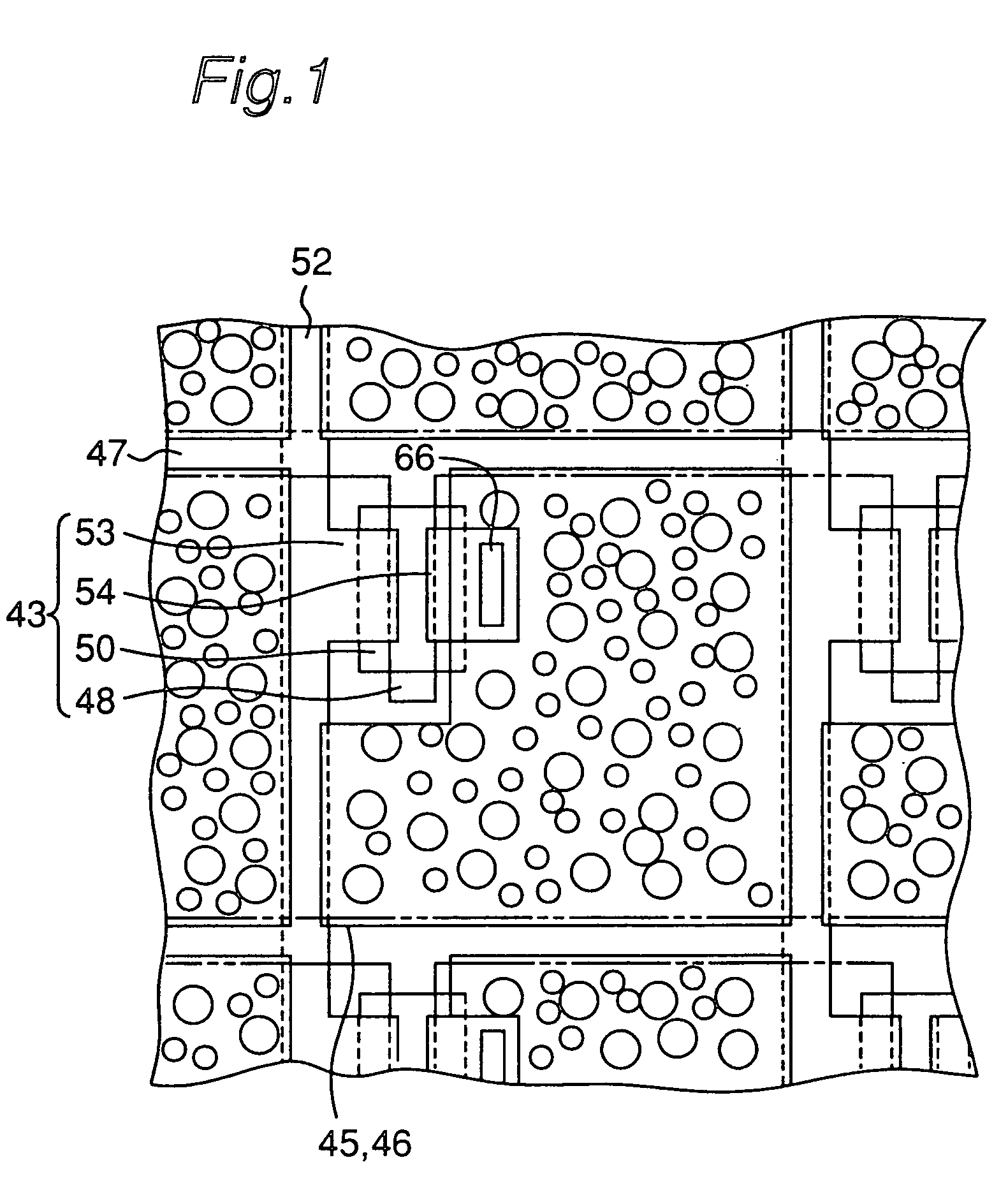
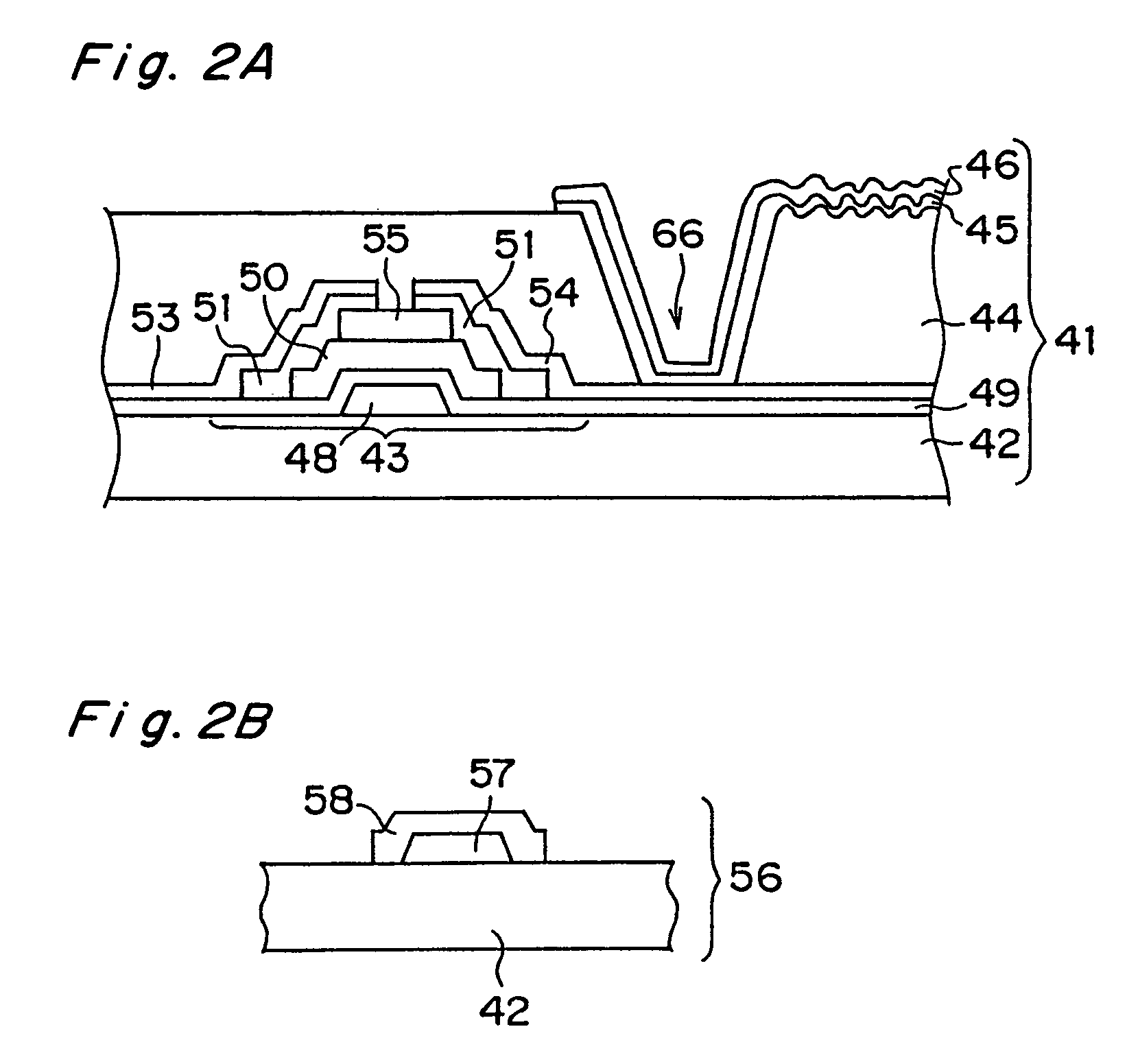
[0042]FIG. 1 is a plan view showing a pixel region of a reflective liquid crystal display as a liquid crystal display of the present embodiment. FIG. 2A is a longitudinal sectional view including a reflective substrate in FIG. 1.

[0043]In the reflective liquid crystal display of this embodiment, as shown in FIG. 2A, a thin film transistor (TFT) 43 for a switching element is formed on an insulating substrate 42 that is composed of glass or the like. Further, a photosensitive resin 44, a MoN film 45 and a reflective electrode 46 are successively formed on the insulating substrate 42 including this TFT to constitute a reflective substrate 41 having smooth concave and convex portions. The photosensitive resin 44 has a function as an interlayer insulating film having concave and convex portions. It is noted that the MoN layer 45 has adhesion and an electrolytic corrosion preventing function. Al forms the reflective electrode 46.

[0044]The TFT 43 is formed by successively laminating a gate ...

second embodiment

[0074]FIG. 7 is a plan view showing a pixel region of a transmissive / reflective liquid crystal display as a liquid crystal display of this embodiment. FIG. 8 is a cross sectional view taken along line A–A′ of FIG. 7.

[0075]In this transmissive / reflective liquid crystal display of the present embodiment, as shown in FIG. 8, a TFT 3 as a switching element is formed on an insulating substrate 2. A photosensitive resin 4 as an interlayer insulating film having concave and convex portions, an MoN film 5 and reflective electrode 6 are successively formed on the insulating substrate 2 including this TFT 3 to constitute a transmissive / reflective substrate 1. Further, a transparent electrode 7 is formed on the insulating substrate 2. It is noted that the MoN layer 5 has adhesion and an electrolytic corrosion preventing function. The reflective electrode 6 is formed out of Al and the transparent electrode 7 is formed out of ITO. The reflective electrode 6 and the transparent electrode 7 consti...

third embodiment

[0093]This embodiment relates to a patterned substrate obtained by forming a MoN interconnect pattern on a resin by utilizing advantages of the MoN.

[0094]FIG. 12 is a partial sectional view of a patterned substrate of this embodiment. A numeral of 71 denotes a PET film. A numeral of 72 denotes an MoN wiring. A numeral of 73 denotes an Mo wiring. The patterned substrate constituted as described above is formed as described below.

[0095]First, the MoN film is formed on the PET film 71 under an atmosphere having a vacuum degree of 0.5 Pa with Ar gas at a flow rate of 100 sccm and N2 gas at a flow rate of 40 sccm. The Mo film is formed under an atmosphere having a vacuum degree of 0.5 Pa with Ar gas at a flow rate of 100 sccm with a thickness of about 1000 Å. Then, photolithography and etching are performed to pattern the MoN film and the Mo film into a prescribed circuit pattern. Thus, the MoN wiring 72 and the Mo wiring 73 are formed.

[0096]A two-layer structure of the MoN wiring 72 and...


PUM

PropertyMeasurementUnit
sizeaaaaaaaaaa
thicknessaaaaaaaaaa
thicknessaaaaaaaaaa

Abstract

A thin film transistor (TFT) is formed on an insulating substrate, and a photosensitive resin film as an interlayer insulating film is formed so as to cover the TFT. Contact holes are formed in the photosensitive resin, and smooth concave and convex portions are provided on an upper surface of the resin. A film including molybdenum nitride (MoN) and a reflective pixel electrode film are successively laminated on the photosensitive resin. The nitrogen content in the MoN film may be between 5 atomic % and 30 atomic % inclusive.

Description

BACKGROUND OF THE INVENTION[0001]The present invention relates to a patterned substrate and a liquid crystal display provided therewith. The patterned substrate referred to herein means an electrically conductive material patterned substrate.[0002]As office automation equipment such as a personal computer and the like has been made portable in recent years, it has become important to manufacture a display device in use for such office automation equipment at a low cost. This display device is formed by interposing a display medium having an electrooptic property between a pair of substrates having electrodes formed thereon. Display is performed by applying a voltage between these electrodes to change the electrooptic property of the display medium.[0003]An active matrix type display device is becoming mainstream because of its display performance. In the active matrix type display device, each pixel is provided with a switching element capable of increasing the number of scanning li...

Claims


Application Information

Patent Timeline
Patent Type & Authority Patents(United States)
IPC IPC(8): C09K19/00G02F1/133G02F1/136G02F1/00G02F1/1333G02F1/1335G02F1/1343G02F1/1362G09F9/30G09F9/35H01L21/77H01L27/12
CPCG02F1/13439G02F1/136286G02F2001/13629G02F2001/136295G02F2201/07G02F2202/28Y10T428/10H01L27/12H01L27/124Y10T428/1059Y10T428/1064Y10T428/1086Y10T428/1095G02F2203/02Y10T428/31678C09K2323/051C09K2323/061C09K2323/05C09K2323/06C09K2323/00G02F1/13629G02F1/136295G02F1/136
Inventor KOKURA, MASAFUMIKATAOKA, YOSHIHARUSHIMADA, TAKAYUKI
Owner SHARP KK
Why Eureka
Try Eureka