Microdisplay pixel cell and method of making it

a technology of micro-display and pixel cell, which is applied in the direction of instruments, semiconductor devices, radio frequency controlled devices, etc., can solve the problems of large limitation of chip size shrinkage, high cost, and defects such as dots or lines to the lcd, so as to reduce the noise of the device, reduce the resistance, and reduce the size of the chip.

Inactive Publication Date: 2006-04-18
UNITED MICROELECTRONICS CORP
View PDF3 Cites 7 Cited by
  • Summary
  • Abstract
  • Description
  • Claims
  • Application Information

AI Technical Summary

Benefits of technology

[0019]It a feature of the present invention that the pixel capacitor is located on the top of the transistor. Thus, the chip size can be greatly shrunk. In addition, both the pixel cap top plate and the pixel cap bottom plate are composed of metal to have a lower resistivity, and the scan line is formed to contacts with the transistor gate directly, therefore the noise of the device can be reduced, the process temperature can be reduced, and the mismatch problem and residue at the edge of the polysilicon electrode as induced in the prior art can be avoided. A linearity for the pixel cap top plate and the pixel cap bottom plate is better when compared to the prior art method. Moreover, since the top plate and the bottom plate for the pixel capacitor is not adjacent to the transistor gate, a coupling effect between them is effectively inhibited and leads to a less possibility for incurring a potential difference. The quality for the transistor gate is more easily controlled since the transistor gate only suffered one etching process in its formation process according to the present invention.

Problems solved by technology

The former one is applied in a large-sized market and still has a gap from widespread application since the technique for mass production is not broken through yet and cost is high.
During the fabrication of the TFT LCD products, however, defects such as dots or lines may occur to the LCD.
Since the pixel capacitor is located at either side of the transistor and occupies the same plane as the transistor according to the prior art design, this design cause a considerable limitation to chip size shrinkage.
In addition, noise of the device cannot be effectively reduced because the length of each metal line in the device cannot be shortened.
Moreover, since both the pixel cap top plate and the pixel cap bottom plate are composed of polysilicon, mismatch and residue problems tend to occur due to the effect of nonuniformity between the etching process and process parameter, such as stop layer.
This results in deviations from the designed electrical performance of the capacitor.
However, new problems still occur.

Method used


Image

  • Microdisplay pixel cell and method of making it
  • Microdisplay pixel cell and method of making it
  • Microdisplay pixel cell and method of making it

Examples


Embodiment Construction

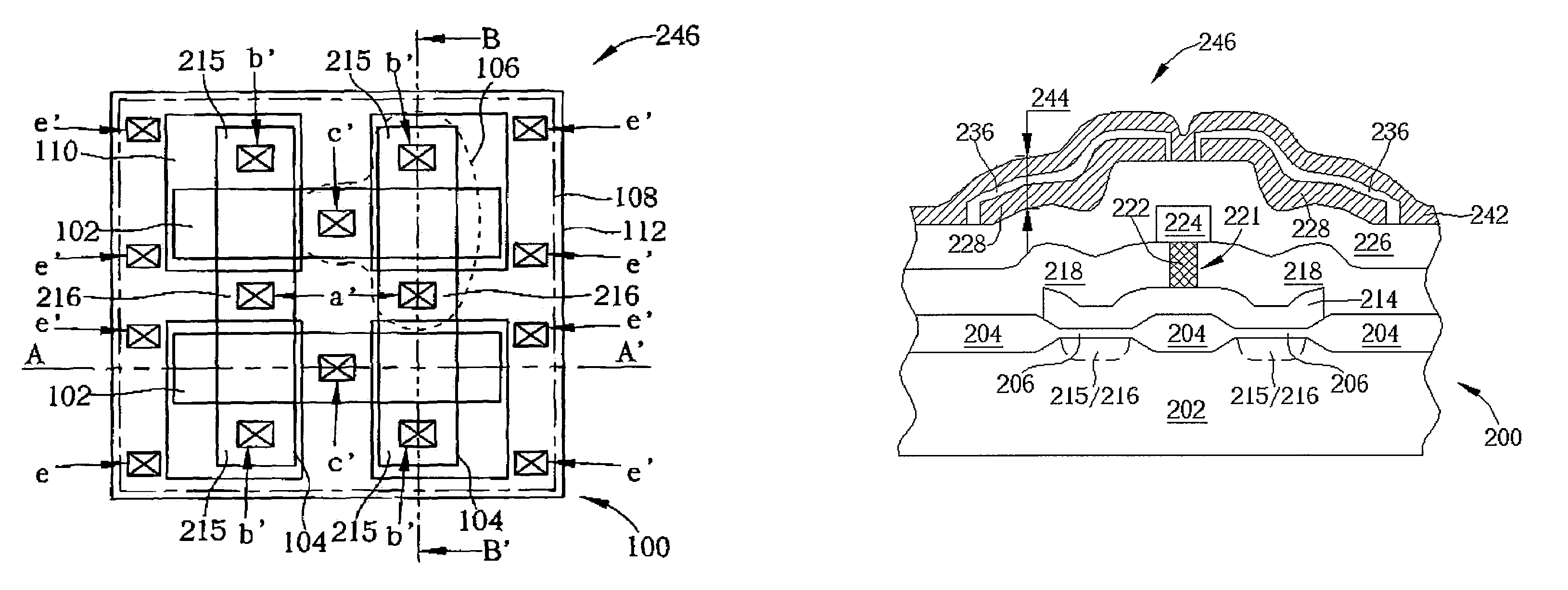
[0025]Please refer to FIG. 8 of a layout of the present invention LCOS display pixel cell 100. The LCOS display pixel cell 100 constitutes a transistor block 108 and a pixel capacitor, including four pixel cap top plates 110 and one pixel cap bottom plate 112, disposed atop the transistor block 108.

[0026]The transistor block 108 further comprises four transistors 106. In other words, the transistor block 108 comprises two polysilicon gates 102 electrically connecting to a word line (not shown). Each polysilicon gate 102 is across two active areas 104. One drain contact plug a″ is formed in each active area 104 for electrically connecting to a video data line (not shown), and two source contact plugs b″ are electrically connected to a pixel cap top plate 110 respectively. One row select contact plug c″ is formed on top of each polysilicon gate 102 for electrically connecting to a row select line, which is the above-mentioned word line. Moreover, the pixel cap bottom plate 112 is elec...


PUM

PropertyMeasurementUnit
pressureaaaaaaaaaa
temperatureaaaaaaaaaa

Abstract

A plurality of active areas are defined on a semiconductor substrate. Then at least one gate is formed on the semiconductor substrate to cover a portion of the active area. Thereafter a plurality of source/drain are formed in the active area not covered by the gate followed by forming a first dielectric layer on the semiconductor substrate to cover the gate and the source/drain. After that, at least one pixel cap top plate is formed atop the first dielectric layer and a capacitor dielectric layer is formed atop the surface of the top plate. Finally, at least one pixel cap bottom plate is formed atop the first dielectric layer to cover the top plate.

Description

BACKGROUND OF INVENTION[0001]1. Field of the Invention[0002]The present invention relates to a microdisplay pixel cell and method of making it, and more particularly, to a pixel cell with a metal-insulator-metal (MIM) capacitor.[0003]2. Description of the Prior Art[0004]In modern planar display technology, plasma display panel (PDP) and liquid crystal display (LCD) are two main streams. They both constitute numerous display grids called as pixel cells. The former one is applied in a large-sized market and still has a gap from widespread application since the technique for mass production is not broken through yet and cost is high. A thin-film transistor LCD (TFT LCD), which is prevailing in recent years, is a representative of the latter one and is mainly applied in the market smaller than 17 inches. During the fabrication of the TFT LCD products, however, defects such as dots or lines may occur to the LCD. Thus, compensate techniques are required to improve the production yields.[0...

Claims


Application Information

Patent Timeline
Patent Type & Authority Patents(United States)
IPC IPC(8): G02F1/1343G02F1/136
CPCG02F1/136G02F1/136277
Inventor CHANG, KUANG-YEHKUO, KUO-YUN
Owner UNITED MICROELECTRONICS CORP
Why Eureka
Try Eureka