Semiconductor integrated circuit and electronic apparatus having the same

a technology of integrated circuits and semiconductors, applied in the direction of printed circuit aspects, sustainable manufacturing/processing, final product manufacturing, etc., can solve problems such as assembly boards and/or ics suffering from heating, and achieve the effect of sufficient bonding strength

Inactive Publication Date: 2005-03-24
ROHM CO LTD
View PDF0 Cites 27 Cited by
  • Summary
  • Abstract
  • Description
  • Claims
  • Application Information

AI Technical Summary

Benefits of technology

[0007] It is therefore an object of the invention to provide a BGA type IC having a multiplicity of reinforcing bumps of substantially the same dimensions as the signal bumps arranged uniformly in the same grid array configuration as the signal bumps, thereby providing the IC with sufficient bonding strength to an assembling board.

Problems solved by technology

The assembly board and / or the IC suffer from heating during the reflow processing, and can be deformed by the heat.
They also suffer from cyclic heating, and hence resultant distortions due to a difference in thermal expansion coefficients between them, while they are in use.
Although use of such reinforcing bumps can improve the mechanical strength, a BGA type IC has a complicated configuration, and hence manufacture of the BGA type IC can entail a new problem to deal with the complexity, since signal bumps and reinforcing bumps have different shapes and different arrangements.

Method used


Image

  • Semiconductor integrated circuit and electronic apparatus having the same
  • Semiconductor integrated circuit and electronic apparatus having the same
  • Semiconductor integrated circuit and electronic apparatus having the same

Examples


first embodiment

[0049] An inventive IC and an inventive electronic apparatus equipped with the IC will now be described in detail by way of example with reference to the accompanying drawings. FIGS. 1 through 4 show the invention.

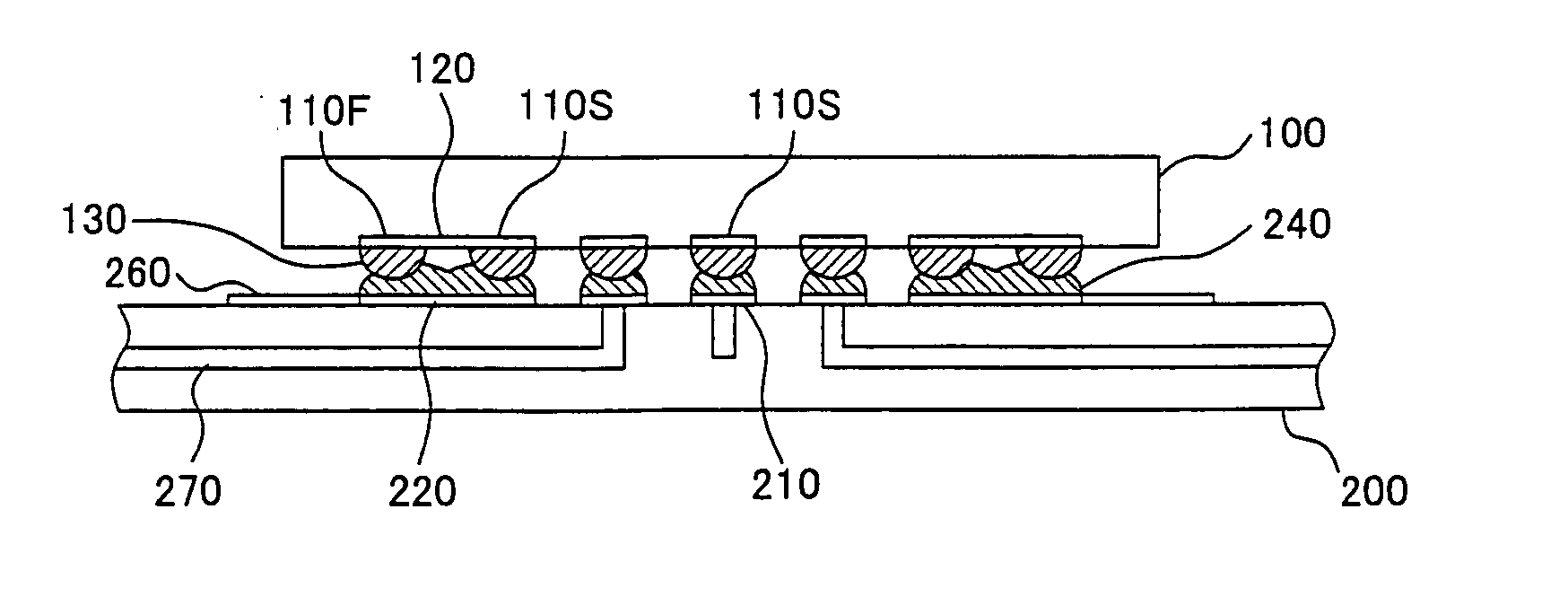
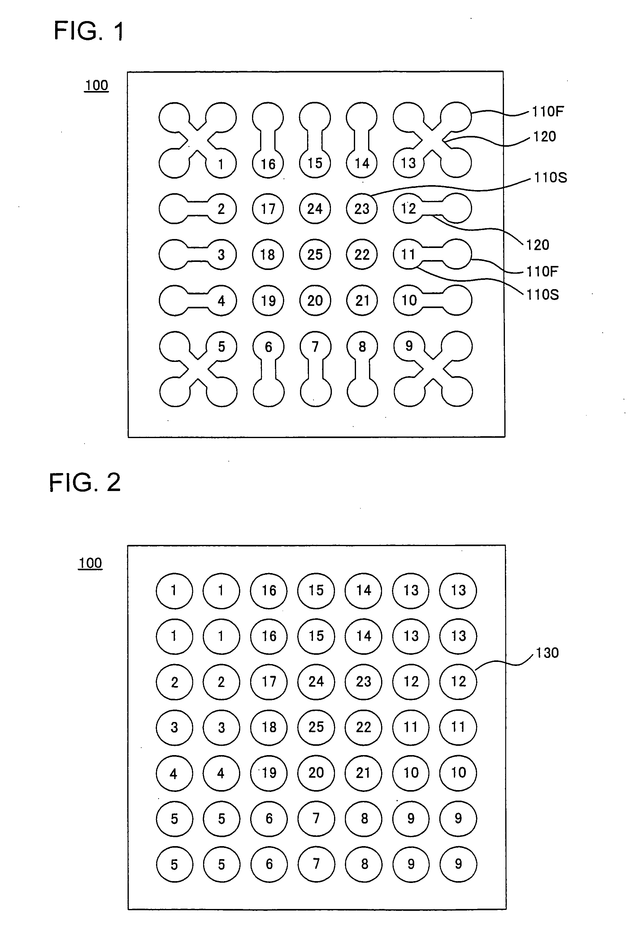
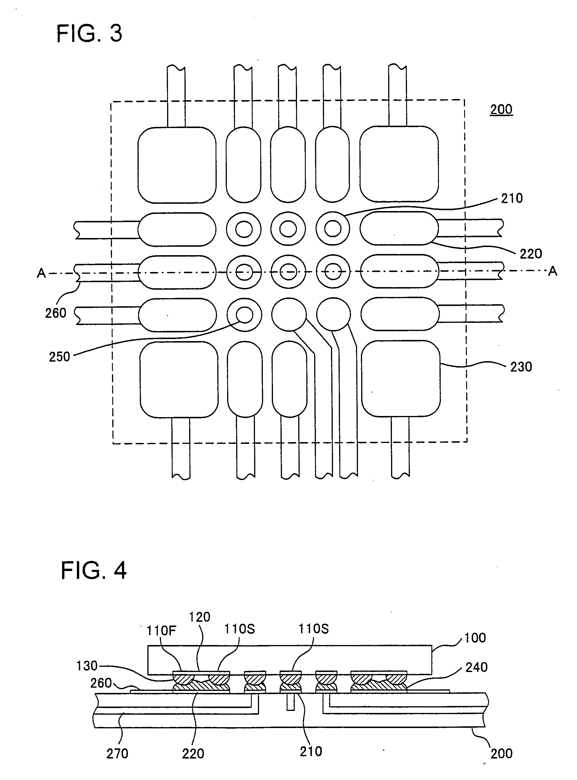
[0050]FIG. 1 shows a grid array pattern of pads arranged on the primary side of the IC. FIG. 2 shows a pattern of bumps formed on the respective pads. FIG. 3 shows a pattern of electrodes (pads) formed on the assembly board for assembling the IC of FIGS. 1 and 2. FIG. 4 shows a schematic sectional view of the IC assembled on the assembly board.

[0051] As shown in FIG. 1, an IC 100 has a multiplicity of pads 110 of substantially the same size arranged in a grid array configuration on a region of the primary side of the IC chip. The region is mostly rectangular in shape, but it can be square as shown in FIGS. 1 and 2. The number of pads 110 is not limited to the number shown in FIG. 1, but is rather arbitrary.

[0052] Of the multiplicity of pads 110 in the grid array, those o...

second embodiment

[0073] Referring to FIGS. 5-7, there is shown the invention. More particularly, FIG. 5 shows a pattern of the pads arranged in a grid array configuration on one primary surface of an IC 100A according to the invention, and FIG. 6 shows a pattern of the bumps formed on the respective pads. FIG. 7 shows an arrangement or pattern of the electrodes formed on the assembly board for assembling the IC of FIGS. 5 and 6.

[0074] In the second example shown, the IC 100A is a grid array type IC which has a multiplicity of pads of substantially the same size arranged in a grid pattern configuration over a rectangular area and a multiplicity of bumps having substantially the same size and formed on the respective pads, as in the first embodiment.

[0075] As shown in FIG. 5, the IC 100A utilizes as the reinforcing pads 110F those pads located on a pair of opposing sides of the array. Each of the reinforcing pads 110F on the two sides is connected to the associated signal pad 110S that lies inside an...


PUM


Abstract

An IC has a multiplicity of electrodes or terminals arranged in a grid array configuration. The IC is provided with a multiplicity of pads in a similar grid array configuration. The pads other than the outermost pads of the array are used as signal pads. The outermost pads are used as reinforcing pads, which are connected to the signal pads adjacent the reinforcing pads. Bumps provided on the reinforcing pads and on the signal pads connected to the reinforcing pads are connected to associated bumps en bloc on an assembly board, thereby allowing the IC to be bonded to the assembly board with sufficient mechanical strength.

Description

FIELD OF THE INVENTION [0001] This invention relates to a semiconductor integrated circuit having a multiplicity of terminals arranged in a grid array configuration, and to an electronic apparatus equipped with such IC. BACKGROUND OF THE INVENTION [0002] Semiconductor integrated circuits (hereinafter referred to as ICs) are mostly packaged to contain an integrated circuit chip. Such IC has electrodes or terminals arranged in, for example, a so-called ball grid array (BGA) structure, in which electrodes are ball-shaped solder bumps arranged in a grid array configuration on one primary side of the IC. ICs having a BGA structure (referred to as BGA type ICs) can be easily equipped with many terminals while keeping substantially the same dimensions as the dimensions of the chip. For this reason, BGA type ICs are called chip-size packages (CSP). BGA type ICs have a further advantage in that an assembly board such as a printed circuit board for assembling thereon the IC only requires subs...

Claims


Application Information

Patent Timeline
Patent Type & Authority Applications(United States)
IPC IPC(8): H01L23/12H01L21/60H01L23/485H01L23/498H01L23/50H05K1/11H05K3/34
CPCH01L23/49816H01L23/49838H01L24/13H01L23/50H01L24/10H01L24/73H01L24/81H01L2224/13099H01L2224/16H01L2224/81801H01L2924/01002H01L2924/01033H01L2924/01079H01L2924/01082H01L2924/14H01L2924/19041H01L2924/19043H05K1/111H05K1/113H05K3/3436H05K2201/094H05K2201/10734H01L2924/01006H01L2924/014H01L24/14H01L2924/00H01L24/05H01L24/06H01L24/09H01L24/16H01L24/17H01L2224/02375H01L2224/05571H01L2224/05573H01L2224/06517H01L2224/09517H01L2224/13H01L2224/14131H01L2224/16227H01L2224/17107H01L2224/17517H01L2924/351Y02P70/50H01L21/60
Inventor NAGAO, ATSUO
Owner ROHM CO LTD
Why Eureka
Try Eureka