Vertical replacement-gate junction field-effect transistor

a technology of junction field and transistor, applied in the field of semiconductor devices, can solve the problems of lithographic process, lithographic process, and current lithographic process nearing the point where it is impossible to accurately manufacture devices at the required minimal size demanded by today's device users, and achieve the effect of higher doping density

Inactive Publication Date: 2006-04-25
BELL SEMICON LLC
View PDF22 Cites 77 Cited by
  • Summary
  • Abstract
  • Description
  • Claims
  • Application Information

AI Technical Summary

Benefits of technology

[0011]A JFET fabricated according to the teachings of the present invention provides a uniform depletion layer (or a uniform pinch-off condition) because the gate completely surrounds the channel and the channel is uniformly doped along a horizontal cross-section. In the prior art, the channel is oriented horizontally and the carriers flow horizontally through it...

Problems solved by technology

However, as the device dimensions shrink, certain manufacturing limitations arise, especially with respect to the lithographic processes.
In fact, current lithographic processes are nearing the point where they are unable to accurately manufacture devices at the required minimal sizes demanded by today's device users.
As the size of these MOSFET devices decreases to achieve increased device density, the fabrication process becomes increasingly difficult.
In particular, the lithographic process for creating the gate channel is problematic, as the wavelength o...

Method used


Image

  • Vertical replacement-gate junction field-effect transistor
  • Vertical replacement-gate junction field-effect transistor
  • Vertical replacement-gate junction field-effect transistor

Examples


Embodiment Construction

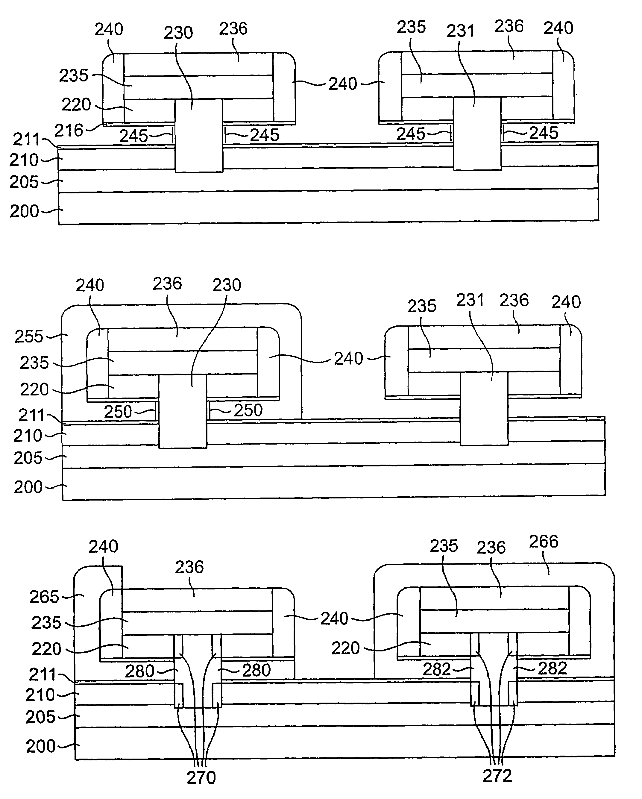
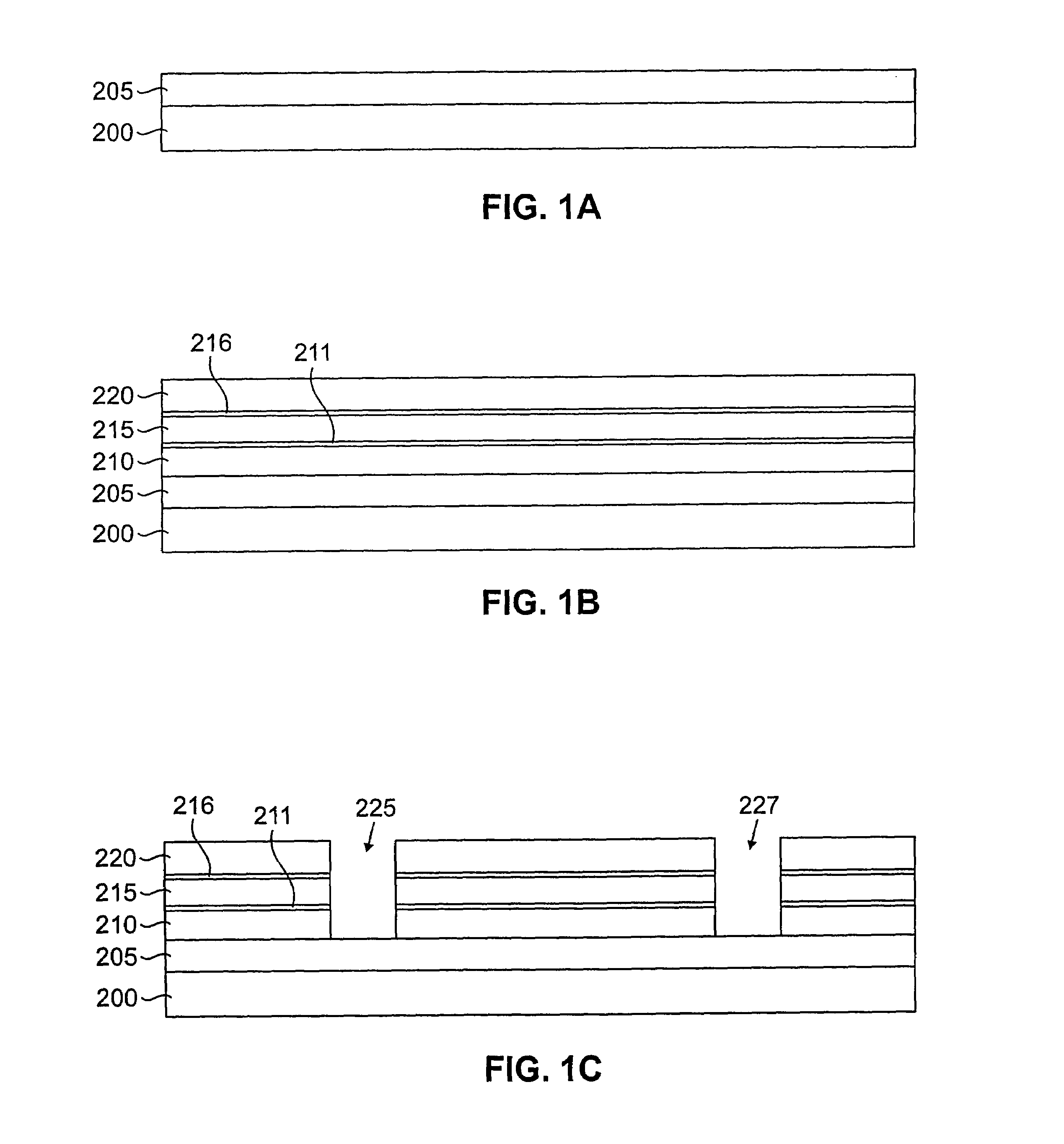
[0015]With regard to the fabrication of transistors and integrated circuits, the term “major surface” refers to that surface of the semiconductor layer in and about which a plurality of transistors are fabricated, e.g., in a planar process. As used herein, the term “vertical” means substantially orthogonal with respect to the major surface. Typically, the major surface is along a plane of a monocrystalline silicon layer on which the field-effect transistor devices are fabricated. The term “vertical transistor” means a transistor with individual semiconductor components vertically oriented with respect to the major surface so that the current flows vertically from source to drain. By way of example, for a vertical JFET the source, channel and drain regions are formed in relatively vertical alignment with respect to the major surface.

[0016]FIGS. 1A through 1R illustrate cross-sectional views of an integrated circuit structure 200 during various stages of fabrication to form an exempl...


PUM


Abstract

An architecture for creating a vertical JFET. Generally, an integrated circuit structure includes a semiconductor area with a major surface formed along a plane and a first source/drain doped region formed in the surface. A second doped region forming a channel of different conductivity type than the first region is positioned over the first region. A third doped region is formed over the second doped region having an opposite conductivity type with respect to the second doped region, and forming a source/drain region. A gate is formed over the channel to form a vertical JFET.
In an associated method of manufacturing the semiconductor device, a first source/drain region is formed in a semiconductor layer. A field-effect transistor gate region, including a channel and a gate electrode, is formed over the first source/drain region. A second source/drain region is then formed over the channel having the appropriate conductivity type.

Description

[0001]This is a Divisional of application Ser. No. 09 / 950,384 filed on Sep. 10, 2001, issued U.S. Pat. No. 6,690,040.FIELD OF THE INVENTION[0002]The present invention is directed to semiconductor devices incorporating junctions of varying conductivity types and methods of making such devices. More specifically, the present invention is directed to vertical replacement-gate (VRG) junction field-effect transistor devices and methods for fabricating integrated circuits incorporating such devices.BACKGROUND OF THE INVENTION[0003]Enhancing semiconductor device performance and increasing device density (the number of devices per unit area), continue to be important objectives of the semiconductor industry. Device density is increased by making individual devices smaller and packing devices more compactly. But, as the device dimensions (also referred to as the feature size or design rules) decrease, the methods for forming devices and their constituent elements must be adapted. For instanc...

Claims


Application Information

Patent Timeline
IPC IPC(8): H01L21/8238H01L21/332H01L21/337H01L21/8232H01L21/8234H01L27/06H01L27/088H01L27/095H01L27/098H01L29/78H01L29/80H01L29/808
CPCH01L21/823487H01L27/088H01L27/098H01L29/42392H01L29/8083H01L29/66742H01L29/66909H01L29/78642H01L29/66545H01L29/7827H01L29/66666H01L29/66893H01L2924/13062
Inventor CHAUDHRY, SAMIRLAYMAN, PAUL ARTHURMCMACKEN, JOHN RUSSELLTHOMSON, ROSSZHAO, JACK QINGSHENG
Owner BELL SEMICON LLC
Why Eureka
Try Eureka