Multi-chamber deposition of silicon oxynitride film for patterning

a silicon oxynitride and patterning technology, applied in chemical vapor deposition coatings, coatings, semiconductor devices, etc., can solve the problems of reducing the thickness of the overlying arc/hardmask, localized non-uniformities in the pecvd silicon oxynitride layer, and dimensional accuracy issues, etc., to achieve accurate dimensioning of device features, enhanced chemical vapor deposition, and improved reliability

Inactive Publication Date: 2006-04-25
GLOBALFOUNDRIES INC
View PDF3 Cites 22 Cited by
  • Summary
  • Abstract
  • Description
  • Claims
  • Application Information

AI Technical Summary

Benefits of technology

[0008]An advantage of the present invention is a method of manufacturing a semiconductor device having improved reliability and accurately dimensioned device features.
[0009]Another advantage of the present invention is a method of manufacturing a semiconductor device comprising transistors with accurately dimensioned sub-micron gate electrodes.
[0010]Additional advantages and other features of the present invention will be set forth in the description which follows and in part will be apparent to those having ordinary skill in the art upon examination of the following or may be learned from the practice of the present invention. The advantages of the present invention may be realized and obtained as particularly pointed out in the appended claims.
[0011]According to the present invention, the foregoing and other advantages are achieved in part by a method manufacturing a semiconductor device, the method comprising: providing a substrate with a patternable layer thereover; forming an amorphous carbon layer over the patternable layer; transferring the substrate to a multi-chamber plasma enhanced chemical vapor deposition (PECVD) apparatus; and sequentially depositing a plurality of silicon oxynitride sub-layers to form a composite silicon oxynitride layer over the amorphous carbon layer.
[0012]Embodiments of the present invention include forming a photoresist mask over the composite silicon oxynitride layer and patterning the underlying patternable layer, such as doped polycrystalline silicon, to form a gate electrode. In accordance with embodiments of the present invention, each silicon oxynitride sub-layer is deposited in an apparatus comprising plural deposition chambers and under conditions such that the density of each silicon nitride sub-layer is at least 2.45 g / cc. Embodiments of the present invention comprise depositing from 2 to 7, e.g., 5, silicon oxynitride sub-layers to form a composite silicon oxynitride layer having a thickness of 300 Å to 700 Å.
[0013]Additional advantages of the present invention will become readily apparent to those skilled in this art from the following detailed description wherein embodiments of the present invention are described simply by way of illustration of the best mode contemplated for carrying out the present invention. As will be realized, the present invention is capable of other and different embodiments, and its several details are capable of modifications in various obvious respects, all without departing from the present invention. Accordingly, the drawings and description are to be regarded as illustrative in nature, and not as restrictive.

Problems solved by technology

As the drive for the continued miniaturization proceeds apace, various issues arise imposing increasing demands for methodology enabling the fabrication of semiconductor devices having accurately dimensioned microminiaturized features.
As the gate width for transistors decreases to about 400 Å and under, various dimensional accuracy issues arise.
However, as the gate width is reduced to 400 A and less, the required reduction in thickness of the overlying ARC / hardmask generates various problems.
For example, when silicon oxynitride is deposited by PECVD over an amorphous carbon layer, residual hydrogen from the amorphous carbon layer is emitted, thereby causing localized non-uniformities in the PECVD silicon oxynitride layer.
The occurrence of pinholes result in at least two serious problems.
One problem generated by pinholes is photoresist poisoning.
Poisoned photoresist exhibits reduced response to conventional photoresist development chemistries and, consequently, remain after development causing undesired patterning of underlying layers during subsequent processing.
Another problem stemming from pinholes is premature etching of the amorphous carbon layer during reworking of the photoresist.
This results in the formation of anomalous patterns in the amorphous carbon layer that may be transferred to underlying layers during subsequent processing.

Method used


Image

  • Multi-chamber deposition of silicon oxynitride film for patterning
  • Multi-chamber deposition of silicon oxynitride film for patterning
  • Multi-chamber deposition of silicon oxynitride film for patterning

Examples


Embodiment Construction

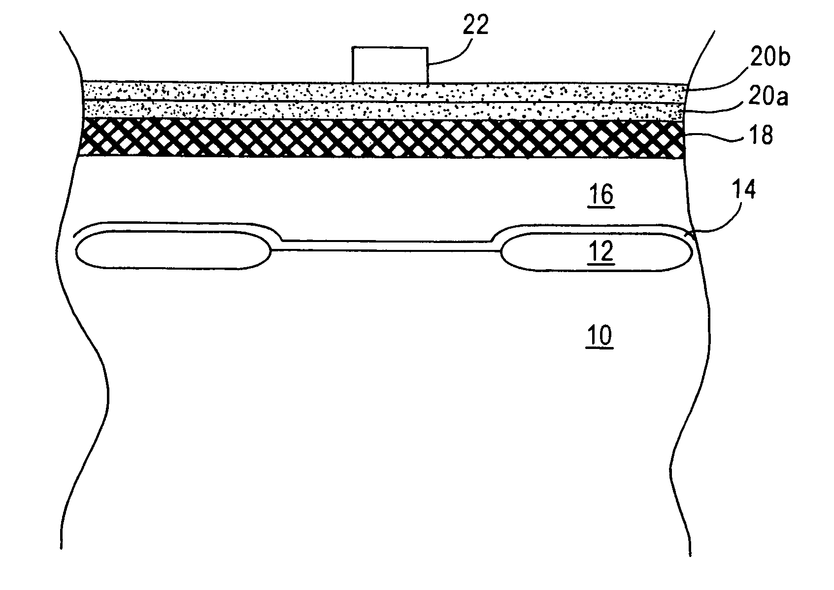
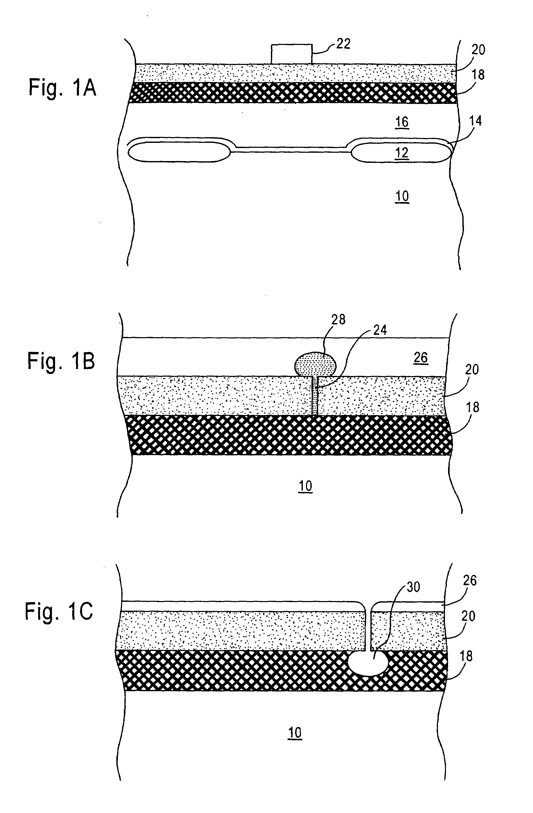
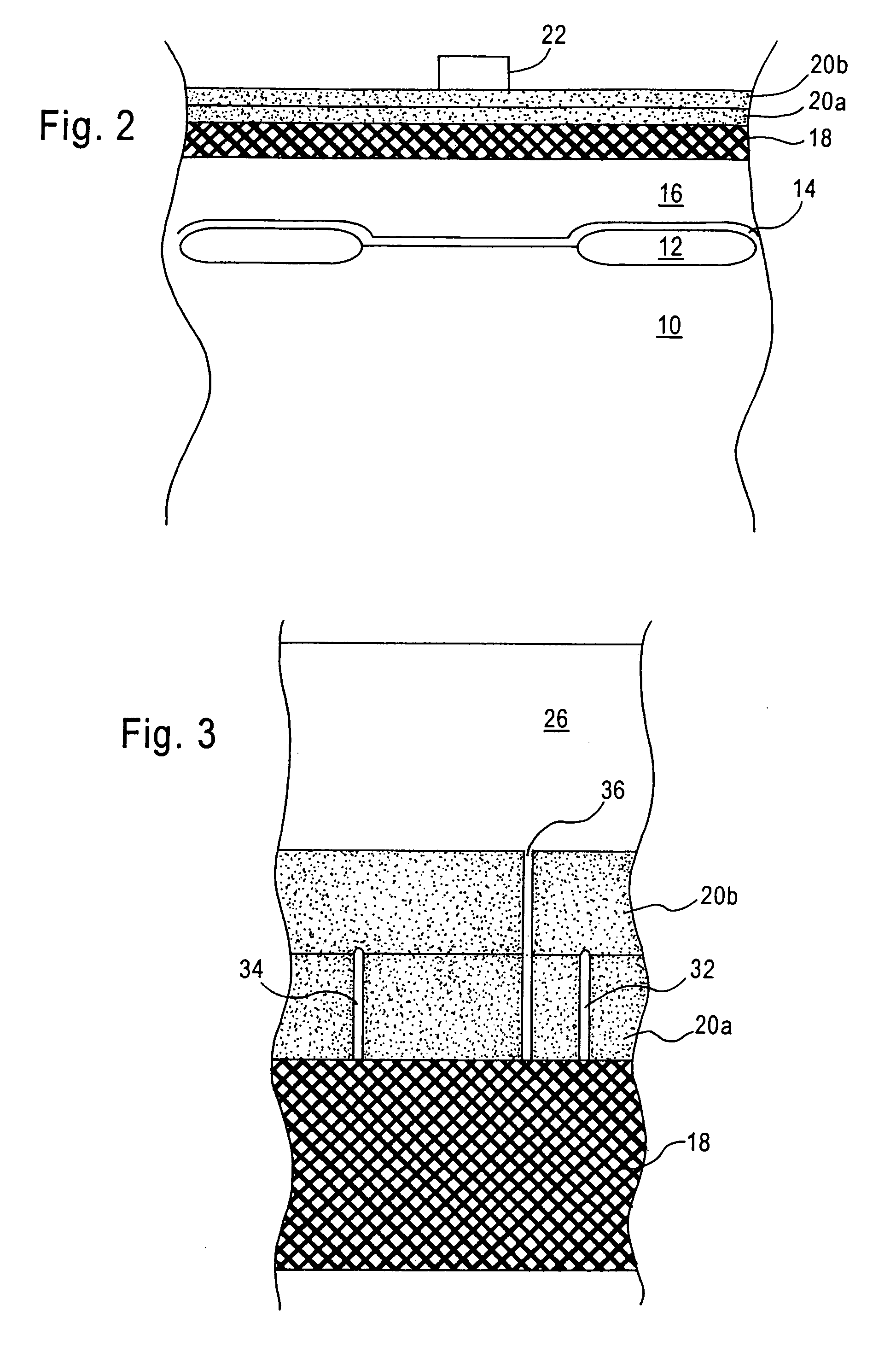
[0018]As semiconductor device feature sizes shrink into the deep-submicron regime, various dimensional accuracy issues arise impacting device reliability. As gate widths plummet to 400 Å and under, it is necessary to reduce the thickness of the ARC / hardmask employed for patterning the gate electrodes. However, such reduction in the ARC thickness generates pinholes causing photoresist poisoning and hardmask etching, thereby adversely impacting the critical dimension.

[0019]These problems were addressed in copending application Ser. No. 10 / 256,368 filed on Sep. 27, 2002 now U.S. Pat. No. 6,803,313, by forming a plurality of silicon oxynitride layers over the amorphous carbon layer. This technique was said to reduce the pinhole density at the surface of the uppermost ARC sub-layer. By providing multiple ARC sub-layers the chance of a pinhole extending from the bottom layer through a line with a pinhole in the top layer was remote. Suitable ARC materials include silicon oxynitride, silic...


PUM

PropertyMeasurementUnit
densityaaaaaaaaaa
densityaaaaaaaaaa
refractive indexaaaaaaaaaa

Abstract

Pinholes in a silicon oxynitride film are reduced by PECVD deposition of a plurality of silicon oxynitride sub-layers in a PECVD apparatus containing multiple chambers. Embodiments include forming a layer of amorphous carbon over a conductive layer, such as doped polycrystalline silicon, on a substrate, transferring the substrate to a multi-chamber PECVD tool and depositing 2 to 7, e.g., 5, sub-layers of dense silicon oxynitride at a total thickness of 300 to 700 Å.

Description

FIELD OF THE INVENTION[0001]The present invention relates to a method of fabricating semiconductor devices exhibiting high reliability, highly accurate device features and superior repeatability. The present invention has particular applicability in fabricating high density, multi-level semiconductor devices with feature dimensions in the deep sub-micron regime.BACKGROUND OF THE INVENTION[0002]As the drive for the continued miniaturization proceeds apace, various issues arise imposing increasing demands for methodology enabling the fabrication of semiconductor devices having accurately dimensioned microminiaturized features. As the gate width for transistors decreases to about 400 Å and under, various dimensional accuracy issues arise.[0003]Semiconductor device features, such as a gate width are typically patterned employing an overlying structure comprising a layer functioning as an anti-reflective coating (ARC) during photoresist patterning and a layer functioning as a hardmask du...

Claims


Application Information

Patent Timeline
Patent Type & Authority Patents(United States)
IPC IPC(8): H01L21/31H01L21/469
CPCC23C16/345H01L21/0332H01L21/32139H01L21/3145Y10S438/95H01L21/3146H01L21/02274H01L21/0214H01L21/02115H01L21/022H01L21/02211
Inventor YOU, LUHUANG, RICHARDGAO, PEI-YUAN
Owner GLOBALFOUNDRIES INC
Why Eureka
Try Eureka