Semiconductor device and method for manufacturing the same

a technology of semiconductors and semiconductors, applied in the direction of coatings, transistors, chemical vapor deposition coatings, etc., can solve the problems of lowering the reliability of elements, increasing leakage current, and reducing film quality

Inactive Publication Date: 2006-04-25
KK TOSHIBA
View PDF12 Cites 5 Cited by
  • Summary
  • Abstract
  • Description
  • Claims
  • Application Information

AI Technical Summary

Benefits of technology

[0018]The present invention has been devised to solve such problems. Specifically, it is an object of the present invention to provide a semiconductor device having a gate insulating film that can minimize both hysteresis and equivalent oxide thickness, and a method for manufacturing such a semiconductor device.

Problems solved by technology

However, since gate leakage current caused by tunnel current will exceed the acceptable value when a SiO2 film is used, the adoption of a new material that can substitute the SiO2 film will be required.
However, since HfO2 has poor heat resistance, there has been a problem of crystallization during the manufacture of a CMOS (complementary MOS), causing increase in leakage current and lowering the reliability of elements.
However, there has been a problem in the HfAlOx film that when the film thickness is reduced, the film quality is lowered.
However, as described above, since the HfSiOx film has a lower specific dielectric constant than the HfAlOx film, there has been a problem that the equivalent oxide thickness cannot be reduced.

Method used


Image

  • Semiconductor device and method for manufacturing the same
  • Semiconductor device and method for manufacturing the same
  • Semiconductor device and method for manufacturing the same

Examples


Embodiment Construction

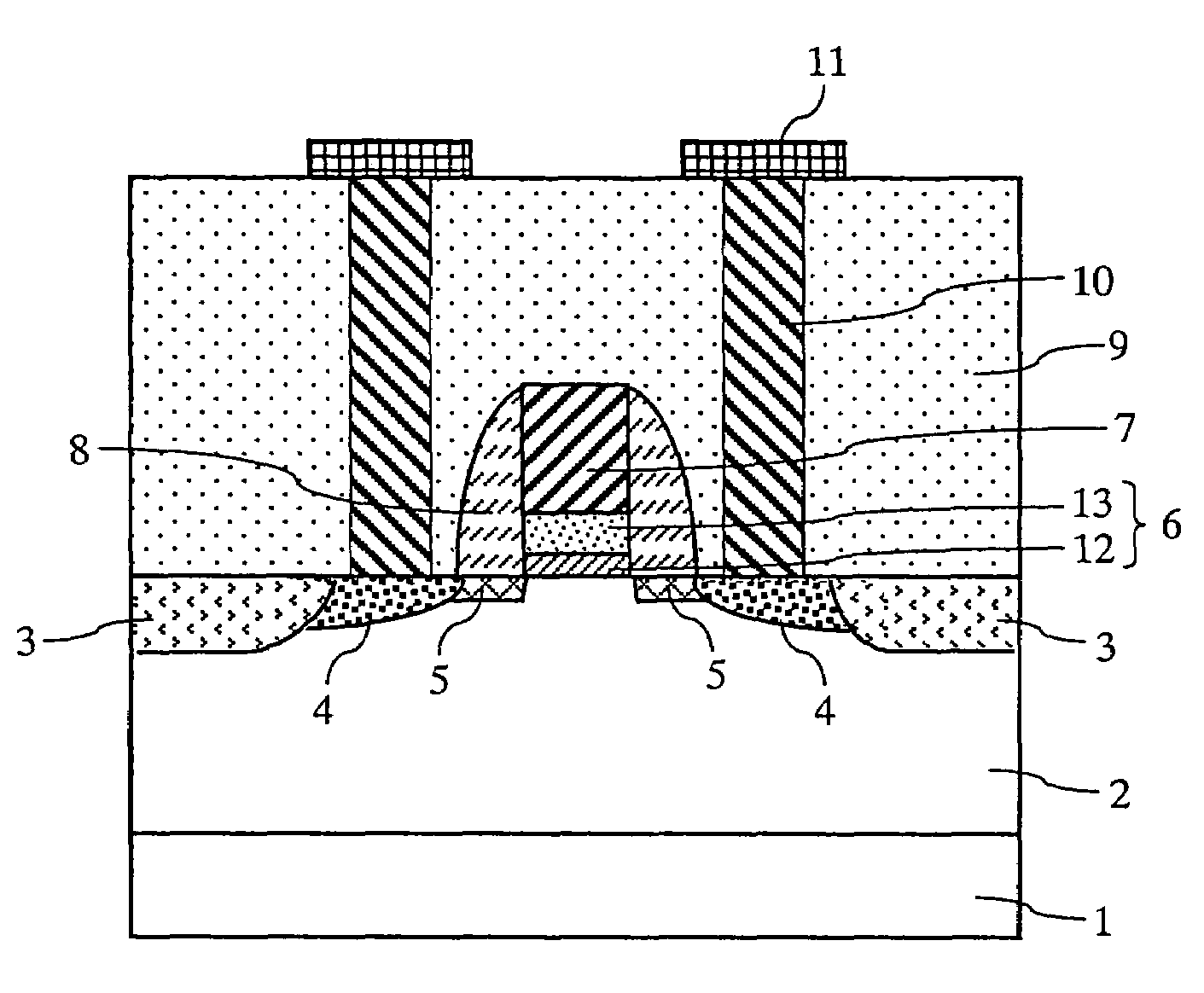
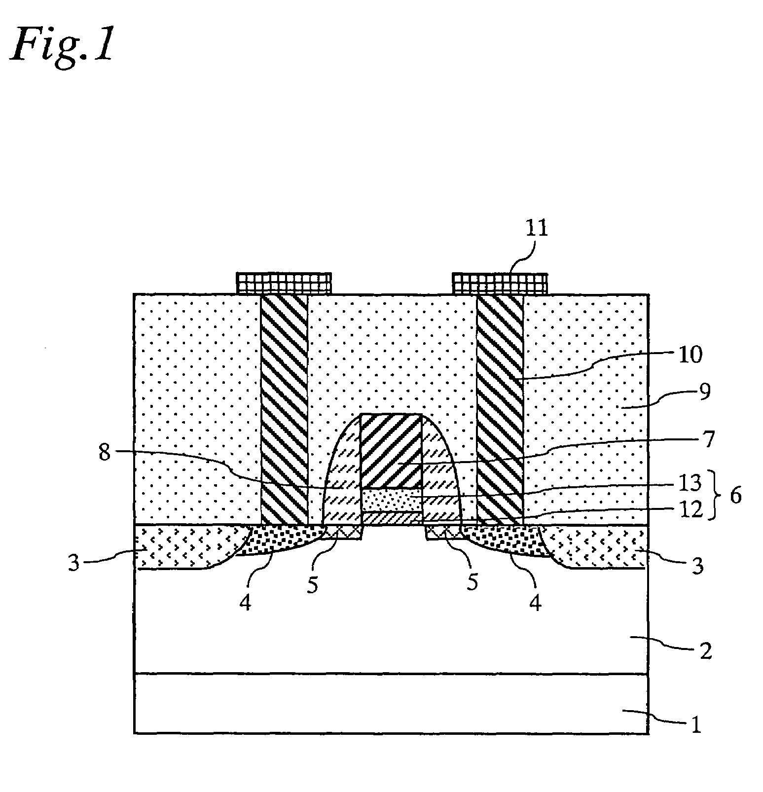
[0041]FIG. 1 is an example of a sectional view of a semiconductor device according to an embodiment of the present invention.

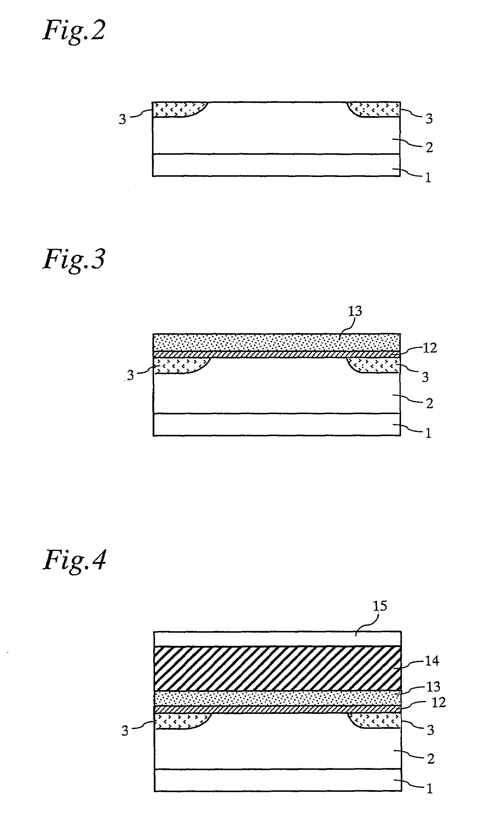
[0042]As FIG. 1 shows, a diffusion layer 2, element-isolating regions 3, source-drain regions 4, and an extension region 5 are formed on a silicon substrate 1. A gate insulating film 6 and a gate electrode 7 are also formed on the silicon substrate 1, and a sidewall 8 is formed on the sides of the gate insulating film 6 and the gate electrode 7. In FIG. 1, the reference numeral 9 denotes an interlayer insulating film, 10 denotes contacts, and 11 denotes wiring layers.

[0043]The gate insulating film 6 is composed of a SiO2 film (silicon dioxide film) 12 and a high-k film (high-dielectric-constant film) 13 formed on the SiO2 film12.

[0044]In this embodiment, a dielectric film containing a transition metal, aluminum (Al), silicon (Si) and oxygen (O). It is especially preferred to use a dielectric film consisting of the mixture of an aluminate and a silicate of a tr...


PUM

PropertyMeasurementUnit
thicknessaaaaaaaaaa
specific dielectric constantsaaaaaaaaaa
surface temperatureaaaaaaaaaa

Abstract

A gate insulating film on a silicon substrate includes a SiO2 film and a high-k film. The high-k film contains a transition metal, aluminum, silicon, and oxygen. The concentration of silicon in the high-k film is higher than the concentrations of the transition metal and aluminum in the vicinity of the interface with the SiO2 film and the vicinity of the interface with the gate electrode. Furthermore, it is preferable that the concentration of silicon is the highest at least in one of the vicinity of the interface with the SiO2 film or the vicinity of the interface with the gate electrode, gradually decreases with distance from these interfaces, and becomes the lowest in a central part of the high-k film.

Description

BACKGROUND OF THE INVENTION[0001]1. Field of the Invention[0002]The present invention relates to a semiconductor device and a method for manufacturing the same; and more specifically, to a semiconductor device that has a gate insulating film formed on a silicon substrate, and a gate electrode formed on the gate insulating film, and method for manufacturing such a semiconductor device.[0003]2. Background Art[0004]In recent years, the high integration in semiconductor integrated circuit devices has significantly proceeded, and in MOS (metal oxide semiconductor) devices, the miniaturization and raising the performance of elements, such as transistors) have been tried. Especially, the reduction of the thickness of a gate insulating film, which is one of elements composing the MOS structure, has rapidly proceeded to cope with the miniaturization, higher-speed and lower-voltage operation of transistors.[0005]As a material for composing a gate insulating film, a SiO2 (silicon dioxide) film...

Claims


Application Information

Patent Timeline
Patent Type & Authority Patents(United States)
IPC IPC(8): H01L29/76C23C16/42H01L21/28H01L21/316H01L21/336H01L29/51H01L29/78
CPCH01L21/28185H01L21/28194H01L29/7833H01L29/517H01L29/513H01L21/18
Inventor ARIKADO, TSUNETOSHIKAWAHARA, TAKAAKITORII, KAZUYOSHIKITAJIMA, HIROSHIMIYAZAKI, SEIICHI
Owner KK TOSHIBA
Why Eureka
Try Eureka