Magnetic storage cell and magnetic memory device using same

a magnetic memory and storage cell technology, applied in semiconductor devices, digital storage, instruments, etc., can solve the problems of large loss of current magnetic field, inability to efficiently carry out the magnetization reversal of each free layer, and inability to form a magnetic path efficiently guiding the current magnetic field, etc., to achieve efficient magnetization reversal, reduce current magnetic field loss, and large storage capacity

Inactive Publication Date: 2006-04-25
TDK CORPARATION
View PDF10 Cites 2 Cited by
  • Summary
  • Abstract
  • Description
  • Claims
  • Application Information

AI Technical Summary

Benefits of technology

[0009]It is an object of the present invention to provide a magnetic storage cell made up of two magneto-resistive elements in a simple structure, which is capable of removing in-phase noise in a read output, reducing a loss of current magnetic field when information is written thereinto to accomplish efficient magnetization reversal, offering a large storage capacity by reducing the area occupied by the magnetic storage cell, and facilitating the manufacturing.

Problems solved by technology

However, in the first to third prior art examples, the magnetization directions of the free layers in a pair of TMR elements, which make up a single magnetic storage cell, are changed by a current magnetic field generated by a plurality of write lines to store information in the magnetic storage cell, but these prior art examples fail to form a magnetic path which efficiently guides the current magnetic field.
Therefore, the conventional magnetic memory devices which have magnetic storage cells, each of which is made up of a pair of TMR cells as in the first to third prior art examples, suffer from a large loss of current magnetic field, and therefore fail to efficiently carry out the magnetization reversal of each free layer.

Method used


Image

  • Magnetic storage cell and magnetic memory device using same
  • Magnetic storage cell and magnetic memory device using same
  • Magnetic storage cell and magnetic memory device using same

Examples


first embodiment

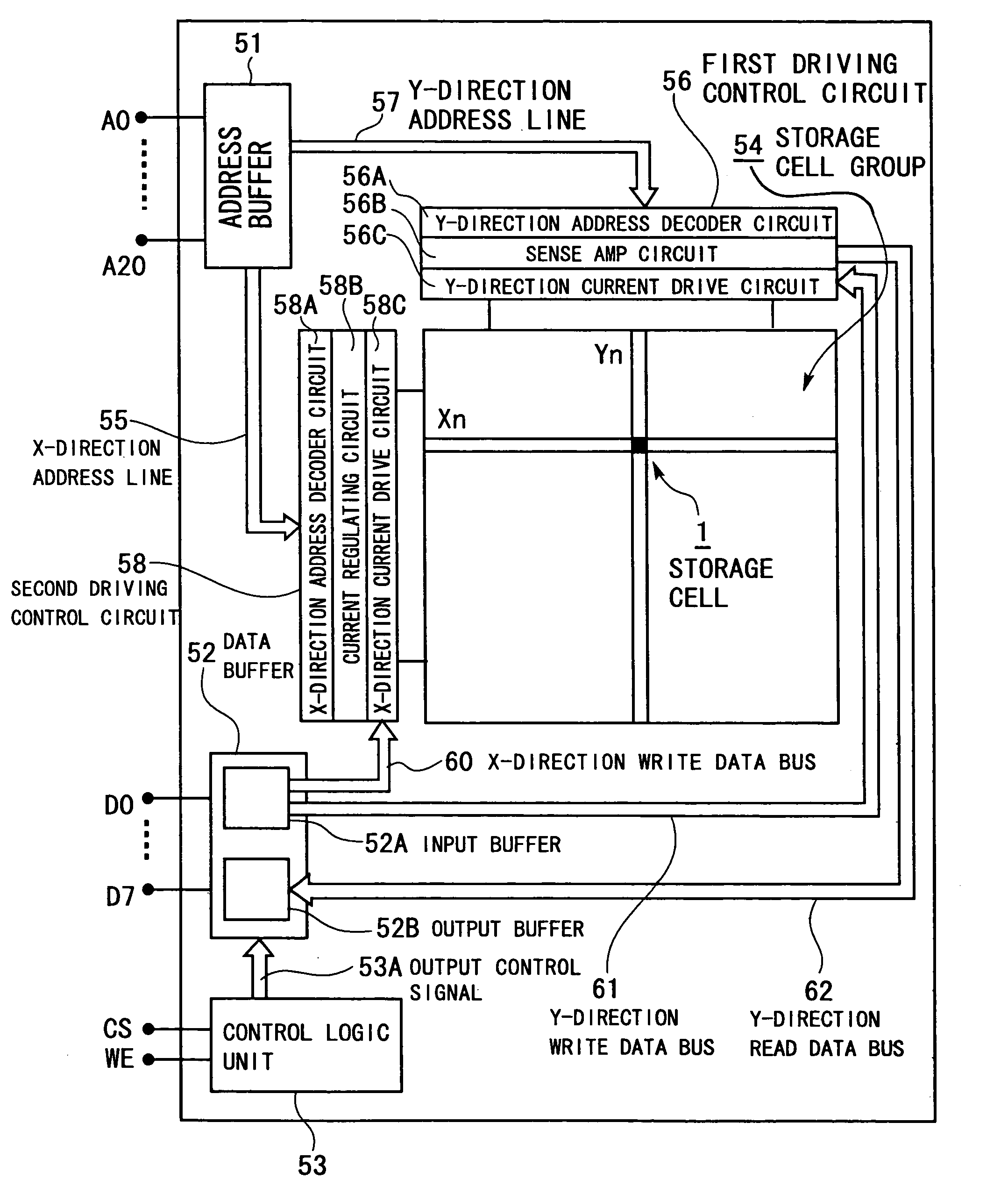
[0103]First, a magnetic memory device according to the present invention will be described with reference FIG. 1 and the like.

[0104]FIG. 1 is a block diagram schematically illustrating the whole configuration of a magnetic memory device according to a first embodiment of the present invention. The magnetic memory device according to the first embodiment comprises components illustrated in FIG. 1 mounted on a semiconductor chip to serve as MRAM.

[0105]The magnetic memory device according to the first embodiment comprises an address buffer 51, a data buffer 52, a control logic unit 53, a storage cell group 54, a first driving control circuit 56, a second driving control circuit 58, external address input terminals A0–A20, and external data terminals D0–D7.

[0106]The storage cell group 54 has a matrix structure in which a multiplicity of storage cells 1, each having two TMR elements (tunneling magneto-resistive elements), arranged in a word line direction (X-direction) and a bit line dir...

second embodiment

[0183]Next, a magnetic memory device according to the present invention will be described with reference FIGS. 37A and 37B.

[0184]FIGS. 37A and 37B are general cross-sectional views schematically illustrating a storage cell 401 of a magnetic memory device according to a second embodiment of the present invention, and correspond to FIGS. 4A and 4B. In FIGS. 37A and 37B, components identical to or corresponding to those in FIGS. 4A and 4B are designated by the same reference numerals, and repetitive description thereon is omitted. This applies to FIGS. 38 to 41, later described.

[0185]The magnetic memory device according to the second embodiment differs from the magnetic memory device according to the first embodiment only in that the storage cell 401 illustrated in FIGS. 37A and 37B is used instead of the storage cell 1 illustrated in FIGS. 4A and 4B.

[0186]The storage cell 401 differs from the storage cell 1 only in that the magnetic layers 21a, 21b are removed from the laminated compo...

third embodiment

[0189]Next, a magnetic memory device according to the present invention will be described with reference FIGS. 38A and 38B.

[0190]FIGS. 38A and 38B are general cross-sectional views schematically illustrating a storage cell 411 of a magnetic memory device according to a third embodiment of the present invention, and correspond to FIGS. 4A and 4B.

[0191]The magnetic memory device according to the third embodiment differs from the magnetic memory device according to the first embodiment only in that the storage cell 411 illustrated in FIGS. 38A and 38B is used instead of the storage cell 1 illustrated in FIGS. 4A and 4B.

[0192]The storage cell 411 differs from the storage cell 1 only in that a bilayer film composed of a lower non-magnetic conductive layer 412b and an upper ferromagnetic layer 413b are added between the ferromagnetic layer 25b and antiferromagnetic layer 26b in the TMR element 2b. The non-magnetic conductive layer 412b can be made of a similar material to that of the non-...


PUM


Abstract

A magnetic storage cell including of two magneto-resistive elements to remove in-phase noise in a read output, and reduces a loss of a current magnetic field, when information is written thereinto, to efficiently produce magnetization reversal. In addition, the area occupied by the magnetic storage cell is reduced to increase the storage capacity, and the structure of the magnetic storage cell is simplified to facilitate the manufacturing. The magnetic storage cell including two TMR elements, and an annular magnetic layer provided commonly for the two TMR elements. The TMR elements are disposed in a direction along a laminating surface with respect to each other. A write bit line and a write word line are provided commonly for the two TMR elements. The annular magnetic layer is disposed with its axial direction defined in a direction along the laminating surface, and is passed through by the lines.

Description

BACKGROUND OF THE INVENTION[0001]The present invention relates to a magnetic storage cell and a magnetic memory device using the same.[0002]Conventionally, in magnetic memory devices such as MRAM (Magnetic Random Access Memory) and the like, magneto-resistive elements such as a TMR element (tunnel magneto-resistive element) and the like are used as magnetic storage cells (see JP-A-2001-236781 and JP-A-2001-266567 (these correspond to U.S. patent application Publication No. 2002 / 0006058.) and the like).[0003]Such magnetic memory devices are exemplified by JP-A-2001-236781 and JP-A-2001-266567 which disclose a plurality types of magnetic memory devices which have magnetic storage cells, each of which is comprised of a pair of TMR elements, and differentially amplify outputs from two TMR elements in pair to generate a read output. In these magnetic memory devices, a write is always performed in a complementary manner such that one of the TMR elements has a free layer (a magnetic layer,...

Claims


Application Information

Patent Timeline
Patent Type & Authority Patents(United States)
IPC IPC(8): G11C11/15G11C11/16H01L21/8246H01L27/105H01L43/08
CPCG11C11/16
Inventor UESUGI, TAKUMIKAGAMI, TAKEO
Owner TDK CORPARATION
Why Eureka
Try Eureka