Semiconductor device and method of manufacturing the same

a technology of semiconductors and semiconductors, applied in semiconductor devices, electrical devices, transistors, etc., can solve the problems of reducing reliability, reducing current gain, and difficult to completely insulate the sub-collector layer, so as to reduce the resistance of the collector and achieve easy planarization. , the effect of expanding the range of materials

Active Publication Date: 2006-05-02
RENESAS ELECTRONICS CORP
View PDF3 Cites 2 Cited by
  • Summary
  • Abstract
  • Description
  • Claims
  • Application Information

AI Technical Summary

Benefits of technology

[0022]In the semiconductor device and the method of manufacturing the same according to this invention, the sub-collector layer is made up of two laminated layers. Thus, the collector resistance can be reduced in the semiconductor device area. To create an element insulating region in the sub-collector layer, ion is implanted into the first layer adjacent to the substrate, and a recess is formed in the second layer where the collector electrode is placed. Since each of the first and second sub-collector layers has half the thickness required for resistance reduction, the ion implantation is ensured, and the planarization is easily achieved because of the low recess height.
[0023]In the case of making up the sub-collector layer only with the first and second sub-collector layers, it is needed to use two different materials having etching selectivity against each other for the first and second layers in consideration of the etching for recess formation. This need can be avoided by inserting the etching stop layer between the first and second sub-collector layers. This expands the range of choices for materials.

Problems solved by technology

If the thickness of the sub-collector layer exceeds the above range, it is difficult to completely insulate the sub-collector layer between elements by ion implantation with boron and so on.
Though the ion implantation with proton, helium and the like allows deep implantation, it degrades reliability.
This poses a problem for the subsequent manufacturing process such as planarization.
If, on the other hand, the doping concentration of the sub-collector layer exceeds the above range, it causes problems such as decrease in current gain and degradation in reliability.

Method used


Image

  • Semiconductor device and method of manufacturing the same
  • Semiconductor device and method of manufacturing the same
  • Semiconductor device and method of manufacturing the same

Examples


first embodiment

[0033]A first embodiment of the present invention is explained hereinafter with reference to FIG. 3.

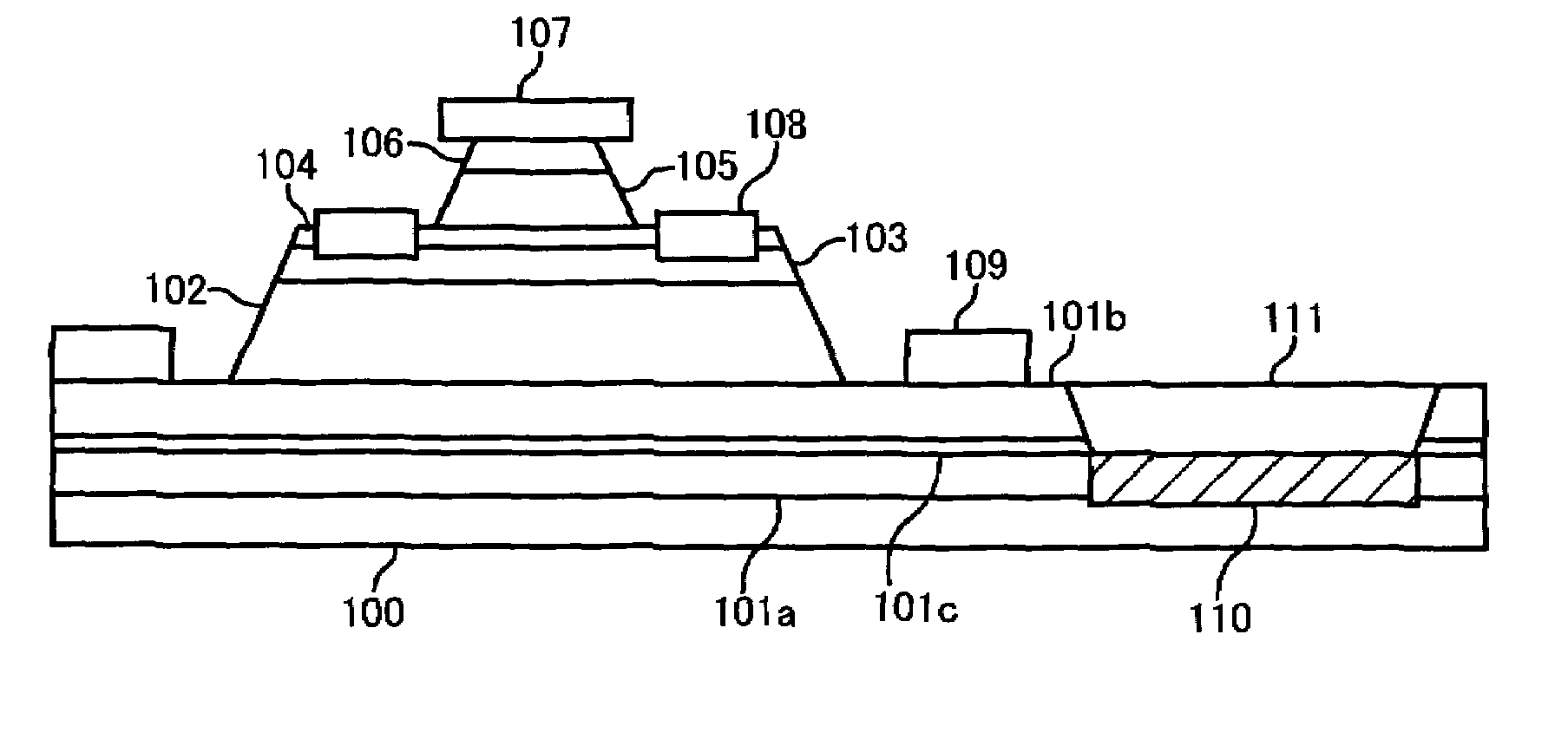
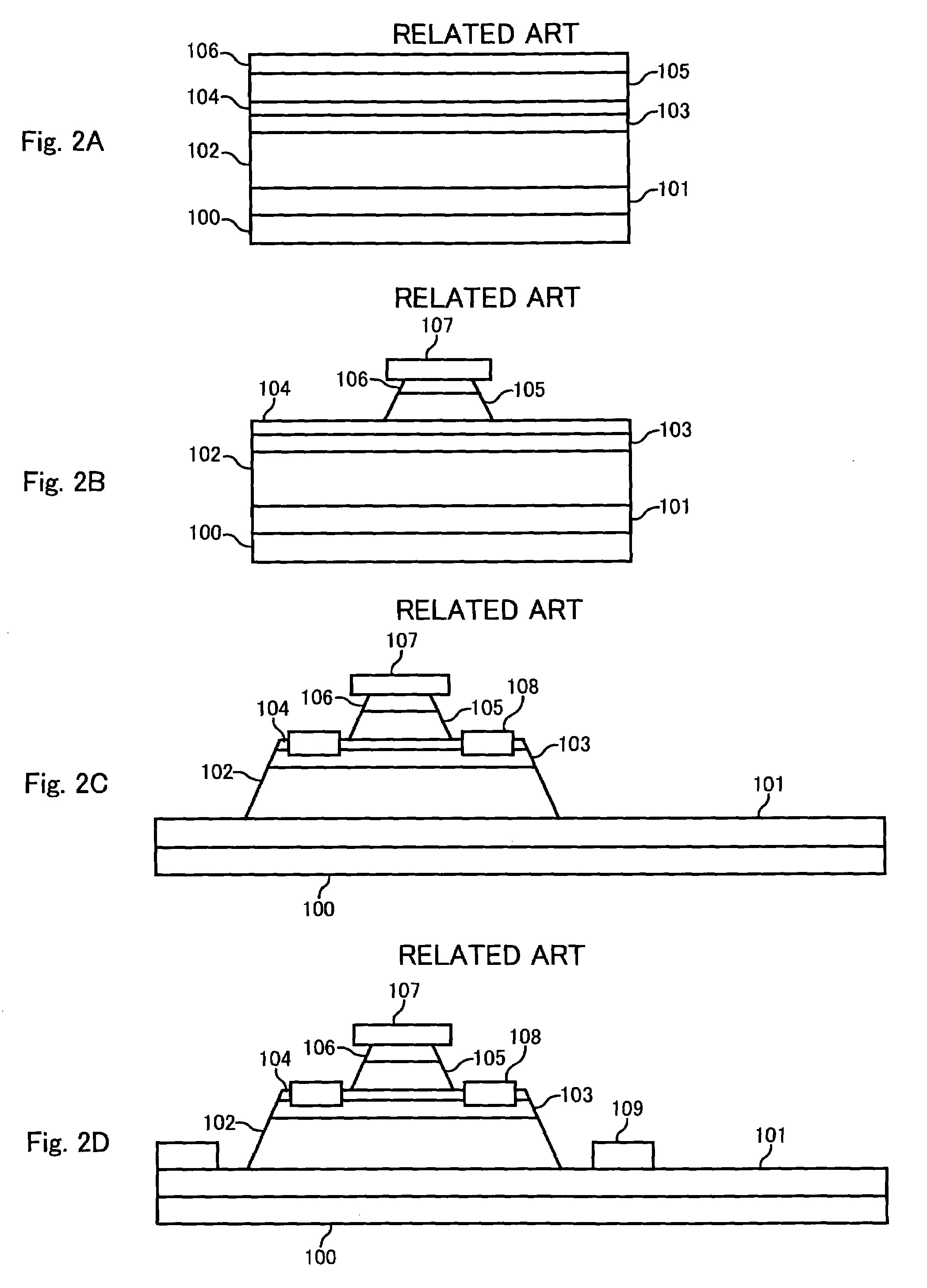
[0034]FIG. 3 is an explanatory view showing an example of the cross section of one device element of the semiconductor device according to the present invention. On a semi-insulating GaAs substrate 100, a first sub-collector layer 101a, an etching stop layer 101c, a second sub-collector layer 101b, a collector layer 102, a base layer 103, an emitter layer 104, an emitter cap layer 105, and an emitter cap layer 106, each having a given shape, are sequentially laminated.

[0035]Unlike the conventional one, the sub-collector layer of this embodiment consists of three laminated layers: the first sub-collector layer 101a at the bottom, the etching stop layer 101c, and the second sub-collector layer 101b at the top. The first sub-collector layer 101a has an element insulating region 110 made by ion implantation. The second sub-collector layer 101b has a recess-shaped element insulating region...

second embodiment

[0047]A second embodiment of the present invention is explained hereinafter with reference to FIG. 5.

[0048]FIG. 5 is an explanatory view showing an example of the cross section of a semiconductor device different from the above-described device. The same elements as in FIG. 3 are denoted by the same reference symbols and redundant description is omitted.

[0049]In this embodiment, the second sub-collector layer 101b only is selectively etched away using the etching stop layer 101c as a stopper, thereby creating the recess-shaped element insulating region 111. The etching stop layer 101c is not etched away. Then, ion implantation with boron and so on is performed both on the exposed etching stop layer 101c and the first sub-collector layer 101a, thereby creating the element insulating region 110 to insulate adjacent device elements from each other.

[0050]This configuration offers substantially the same effect as the above embodiment.

third embodiment

[0051]A third embodiment of the present invention is explained hereinafter with reference to FIG. 6.

[0052]FIG. 6 is an explanatory view showing an example of the cross section of a semiconductor device different from the above-described devices. The same elements as in FIG. 3 are denoted by the same reference symbols and redundant description is omitted.

[0053]This embodiment is different from the above embodiment in that it eliminates the etching stop layer.

[0054]Thus, the first sub-collector layer 101a is made of the material which has etching selectivity against the second sub-collector layer 101b.

[0055]For example, the first sub-collector layer 101a is formed of GaAs, and the second sub-collector layer 101b is formed of AlGaAs, InGaP, or InGaAsP. For another example, the first sub-collector layer 101a is formed of AlGaAs, and the second sub-collector layer 101b is formed of InGaP or InGaAsP. For still another example, the first sub-collector layer 101a is formed of InGaAs, and t...


PUM


Abstract

A semiconductor device includes a sub-collector layer, a collector layer, a base layer, an emitter layer, and an emitter cap layer, which are sequentially laminated on a substrate. It also includes an emitter electrode, a base electrode, and a collector electrode, which are respectively formed on the emitter cap layer, the base layer, and the sub-collector layer. The sub-collector layer is made up of a first sub-collector layer adjacent to the substrate and a second sub-collector layer adjacent to the collector layer. In the area between adjacent device elements, the first sub-collector layer has an element insulating region created by ion implantation, and the second sub-collector layer has a recess-shaped element insulating region.

Description

BACKGROUND OF THE INVENTION[0001]1. Field of the Invention[0002]The present invention relates to a semiconductor device such as heterojunction bipolar transistor (HBT) and a method of manufacturing the same. Particularly, the present invention relates to a semiconductor device which ensures electrical isolation between device elements such as HBT and easily achieves high current gain, high reliability, and planarization while reducing collector resistance to enhance the efficiency of an amplifier, and a method of manufacturing the same.[0003]2. Description of Related Art[0004]A typical example of HBT is fabricated on a semi-insulating gallium arsenide (GaAs) substrate. A sub-collector layer, a collector layer, a base layer, an emitter layer, and an emitter cap layer are epitaxially grown on the semi-insulating GaAs substrate. Further, an emitter electrode, a base electrode, and a collector electrode are respectively formed on the emitter cap layer, the base layer, and the sub-collec...

Claims


Application Information

Patent Timeline
Patent Type & Authority Patents(United States)
IPC IPC(8): H01L29/22H01L31/0328H01L21/265H01L21/331H01L21/76H01L21/8222H01L27/082H01L29/737H01L29/739
CPCH01L29/7371H01L29/66318
Inventor ISHIGAKI, TAKASHINIWA, TAKAKIKUROSAWA, NAOTOSHIMAWAKI, HIDENORI
Owner RENESAS ELECTRONICS CORP
Why Eureka
Try Eureka