

Semiconductor device and method for manufacturing the same
a semiconductor and device technology, applied in the direction of semiconductor devices, microlithography exposure apparatus, electrical apparatus, etc., can solve the problem of reducing the dimension of the device any mor
- Summary
- Abstract
- Description
- Claims
- Application Information
AI Technical Summary
Benefits of technology
Problems solved by technology
Method used
Image

Examples
first embodiment
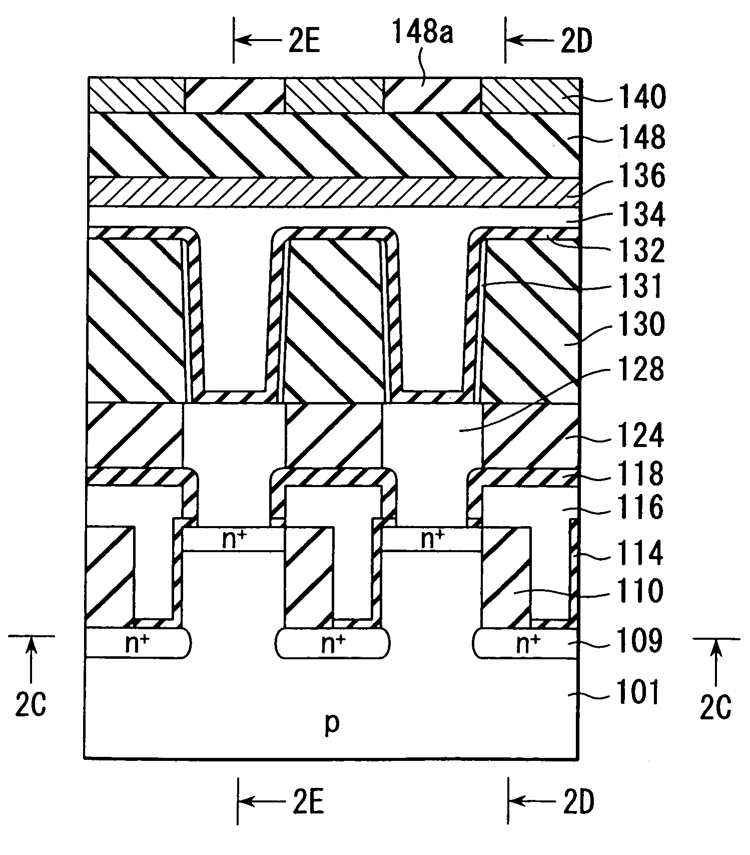
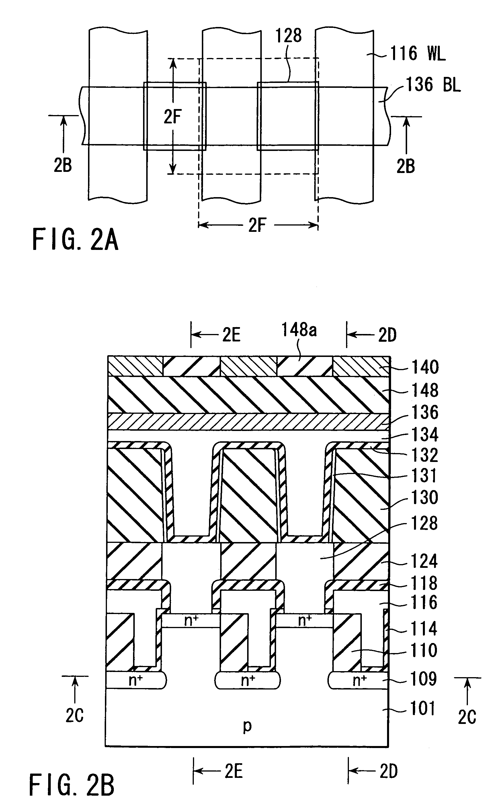
[0077]FIG. 2A is a view showing a planar layout of a memory cell according to a first embodiment of the present invention with mask patterns set in an aligned state as a model layout. FIG. 2B is a cross-sectional view along the line 2B—2B in FIG. 2A. A transistor used for the memory cell of the first embodiment is formed as a vertical type. That is, in FIG. 2B, one of source and drain (impurity layer) 109 is formed at an upper surface of a semiconductor substrate 101 and the other is formed at the bottom of a trench formed on the lower portion of a word line 116. The gate electrode is formed on a side surface of the trench and forms a portion of the word line 116. Above the source / drain layer 109 having a planar configuration at the upper surface of the substrate, a capacitor is formed substantially aligned with that planar configuration. By arranging them in such a way, a memory cell is realized which has a cell area given by 4F2 of “2F in length×2F in width” as shown in FIG. 2A.
[0...
second embodiment
[0099]FIGS. 16A and 16B are a planar layout diagram, and a cross-sectional view, showing a memory cell as a model according to a second embodiment of the present invention. The memory cell of the second embodiment has a configuration of an occupation area 4F2 also and is comprised of a capacitor coupled bit-line cell structure. This configuration is different from that of the first embodiment in respect of the source / drain dimension of its vertical type transistor and its manufacturing method. Now an explanation will be made below about the manufacturing method. For easiness in understanding of this embodiment, the same reference numerals are employed to designate the same portions or areas corresponding to those shown in the first embodiment.
[0100]First, a silicon column 106 as shown in FIG. 17 is formed in the same way as the first embodiment of FIG. 4A. That is, after an about 10 nm buffer oxide film 102 has been formed on the surface of a p type silicon substrate 101, an about 2...
third embodiment
[0110]A memory cell of the third embodiment has the same equivalent circuit as that of the prior art shown in FIG. 1A and is of such a type that a constant voltage is applied to the plate electrode of a capacitor. In this case, however, a so-called surrounding gate type vertical transistor is used where the side surfaces of the silicon column are all surrounded with a gate electrode and a bit line formed at the upper side of the silicon column is connected to a trench bottom through a plug.
[0111]FIGS. 26A and 26B are a planar layout diagram, and a cross-sectional view, of a memory cell according to the third embodiment of the present invention. Even if this structure is adopted, it is possible to realize a memory cell of an occupation area 4F2. An explanation will be made about the manufacturing process of this memory cell. For ease in understanding of the embodiments, the same reference numerals are employed to designate portions or areas corresponding to those shown in the first e...
PUM
 Abstract
Description
Claims
Application Information