High-frequency active inductor

a high-frequency active inductors and active inductors technology, applied in the field of integrated circuits, can solve the problems of increasing the phase shift of the transconductors, severely reducing the useable frequency range, and intrinsically very lossy transistors

Inactive Publication Date: 2006-05-09
PORTLAND STATE UNIV
View PDF5 Cites 43 Cited by
  • Summary
  • Abstract
  • Description
  • Claims
  • Application Information

AI Technical Summary

Benefits of technology

[0042]A differential pair of transistors M1 and M2 corresponds to the non-inverting transconductor gm1 12 of FIG. 1A, and a transistor M3 corresponds to the inverting transconductor gm2 14 of FIG. 1A. The signal path propagates through nodes 1, 2, and 3, and preferably includes only NMOS transistors. In accordance with Eq. (1), the parasitic capacitance at node 3 is gyrated to form an inductance by transistors M1, M2, and M3. The inductance and parasitic capacitance at node 1 form a resonator, having the resonance frequency fR shown in Eq. (2). Node 2 has an advantageous parasitic capacitor that, as described below, can be used to compensate for the large output conductance (source-drain leakage gds) of submicron MOSFETs that cause the gyrator to be lossy. Therefore, structure of active inductor circuit 32 is very efficient.
[0043]Active inductor circuit 32 of this invention is advantageous because it employs only three NMOS transistors in its signal path to increase the maximum operating frequency by 40%, up to 7 gHz (for 0.2 micron technology) in simulation and 5.7 gHz in experiment. This high-frequency performance is possible because the mobility of NMOS is four to five times greater than PMOS in submicron CMOS technologies.

Problems solved by technology

The multiple-transistor transconductors with linearization employed in transconductor-capacitor (Gm-C) filters can not generally be used here, because their internal nodes generate parasitic poles, which increase the phase shift of the transconductors and severely reduce their useable frequency range.
Modern submicron CMOS technology having a minimum transistor length L less than 1 μm brings quite a few challenges to active inductor designers.
Among them: the transistors are intrinsically very lossy because of the short-channel effect, the supply voltage is low (≦1.8 V), the threshold voltages (VTs) are relatively high (0.5–0.7 V), and metal-insulator-metal (MiM) capacitors are not available in standard digital CMOS technologies.
However, subject to the constraints of dc biasing and device characteristics, prior methods for constructing CMOS active inductors are very limited.
M1 serves as the non-inverting transconductor within the gyrator, but is not very efficient because of its common-drain arrangement.
However, this reduces the dynamic range of the circuit, and may be impossible to implement in low-voltage submicron technology.
However, this approach also has an intrinsically low-Q because a node between the two transistors is connected to the source of the top NMOS device and has very low impedance.
A negative resistor is added to the circuit to enhance Q, but this undermines the frequency benefits that the simple structure may offer.
As a result, the final circuits are complex and the maximum operating frequency is reduced.
While working-around and solving some of the above-described problems, the prior active inductor structures using submicron CMOS technologies nevertheless exhibit several disadvantages:a. The number of transistors employed in the prior circuits is typically large (four to nine or greater), and the operating frequency is limited to 1–2 gHz with submicron fabrication technologies, because the signal path contains too many nodes and hence multiple parasitic poles.
The negative resistor increases the noise and parasitic capacitance of the circuit.
The cascode structure limits the dynamic range and is not compatible with low-voltage (≦1.8 V) operation.
To reduce the circuit loss in these structures, the transistor lengths are usually 2–3 times the technology minimum, so that the high-speed advantage of submicron technology cannot be fully exploited.
Many prior designs employ costly modified CMOS technologies to derive components normally not available in standard digital CMOS technologies, such as MiM capacitors, or to enhance the characteristics of CMOS transistors, such as lowering VT.

Method used


Image

  • High-frequency active inductor
  • High-frequency active inductor
  • High-frequency active inductor

Examples


Embodiment Construction

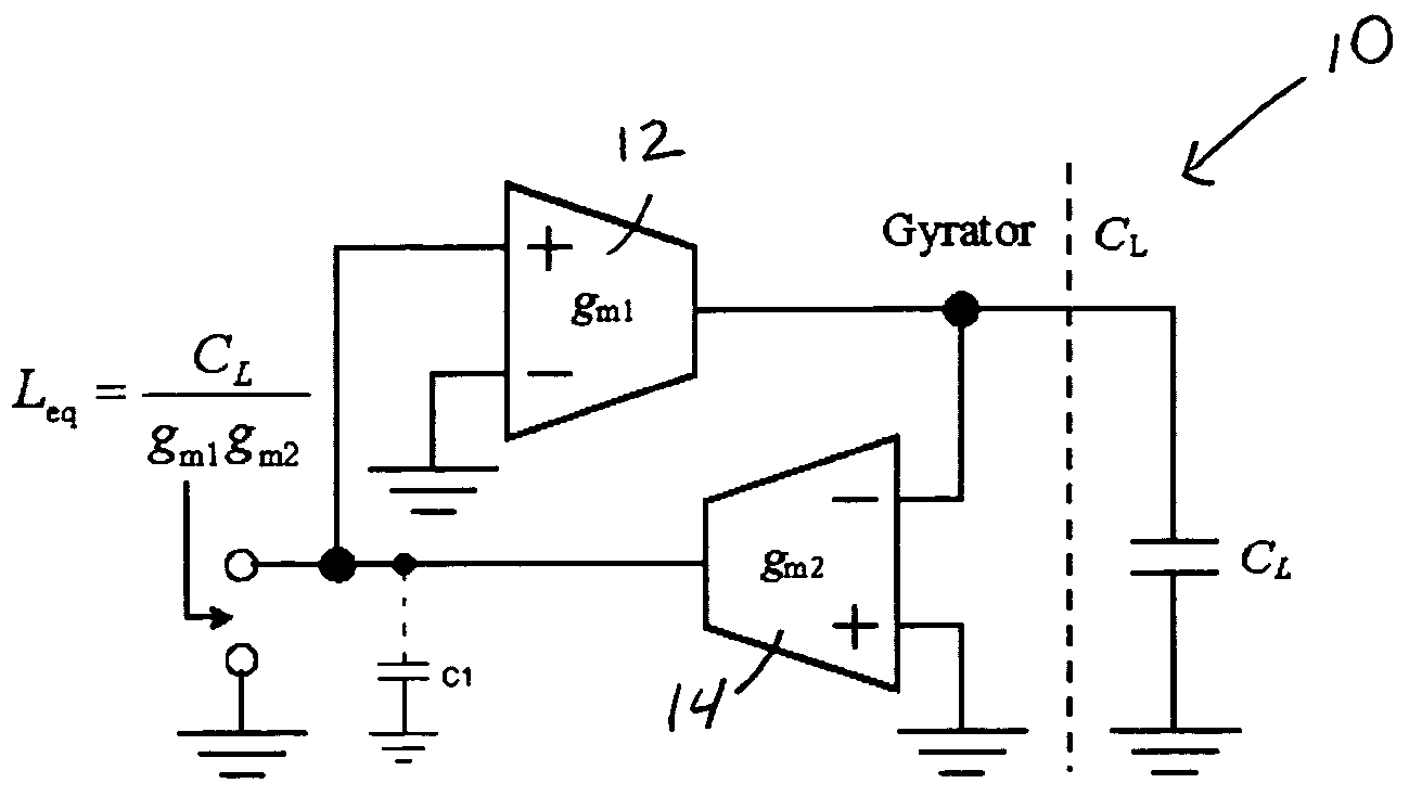
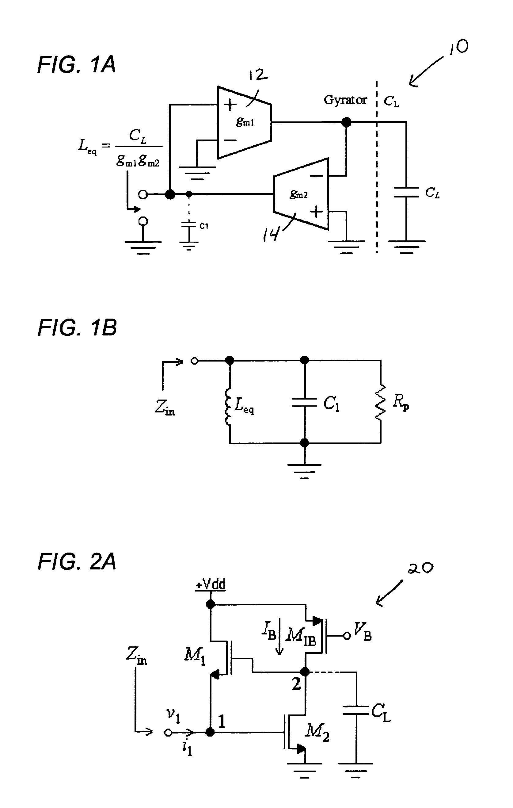
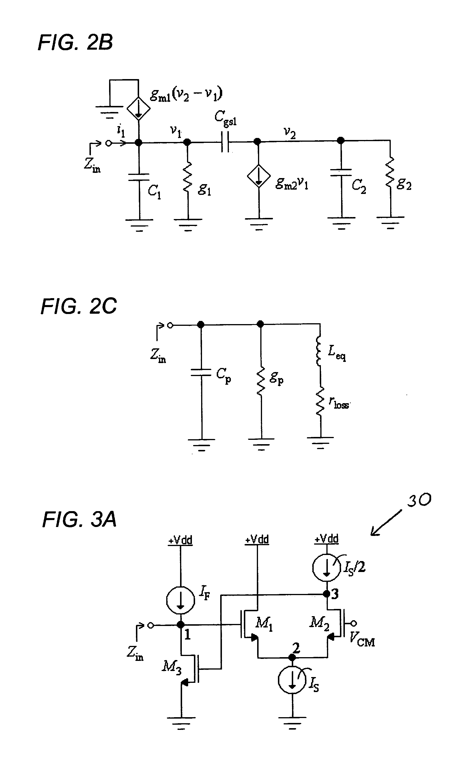
[0054]Referring to FIGS. 4A and 4B, a mathematical small-signal analysis is set forth below to demonstrate the performance of active inductor circuit 32. FIG. 4A shows a small-signal equivalent circuit 40 of active inductor circuit 32. A conductance g1 represents the sum of drain-source leakage gds from M3 and MIF, and a conductance g3 represents primarily the drain-source leakage gds of MIS / 2. A capacitor C1≈0.5Cgs1+Cjd3+Cjd,IF+CL, where Cjd,IF represents the drain diffusion capacitance of transistor MIF, and CL represents the load capacitance (including the input capacitance of any subsequent circuitry). A capacitor C3≈Cgs3+Cjd2+Cjd,IS / 2, where Cjd,IS / 2 is the drain-diffusion capacitance of transistor MIS / 2. A transconductor Gm2=gm3, the transconductance of transistor M3. A transconductor Gm1 has an internal node, and its small-signal equivalent circuit 42 is represented by FIG. 4B.

[0055]In FIG. 4B, a conductance g2≈gds,IS+gds1, where gds,IS is the gds of transistor MIS. A capacit...


PUM


Abstract

An active inductor circuit implemented in sub-micron CMOS semiconductor technology is usable at gigaHertz frequencies and includes an input node, a non-inverting transconductor circuit comprising a differential pair of NMOS transistors connected to the input node, an inverting transconductor circuit comprising an NMOS transistor connected to an output node of the non-inverting transconductor circuit and connected to the input node in a gyrator feedback configuration. Varactors coupled to the transconductor circuits tune the frequency and Q of the active inductor circuit.

Description

RELATED APPLICATION[0001]This application claims the benefit of U.S. Provisional Application No. 60 / 501,584, filed Sep. 8, 2003, which is incorporated herein by reference.FEDERALLY SPONSORED RESEARCH OR DEVELOPMENT[0002]Not applicable.TECHNICAL FIELD[0003]This application relates to the field of electronic circuits and, in particular, to integrated circuit (IC) methods and circuits for implementing active inductors.BACKGROUND OF THE INVENTION[0004]An integrated inductor capable of operating at gigaHertz (109 Hz) frequencies is a critical element in, e.g., oscillators, filters, and wide-band low-noise amplifiers (LNAs). The main applications are radio-frequency (RF) communication and high-speed data processing ICs, such as those in cellular phones, wireless network cards, and broadband transceivers.[0005]Integrated inductors may be classified as passive or active. Most passive integrated inductors are implemented by metal wires in spiral form, hence the name “spiral inductors.” Other...

Claims


Application Information

Patent Timeline
Patent Type & Authority Patents(United States)
IPC IPC(8): H03H11/00H03F3/45H03H11/48
CPCH03H11/486H03H11/48H03H11/50
Inventor XIAO, HAIQIAOSCHAUMANN, ROLFDAASCH, W. ROBERT
Owner PORTLAND STATE UNIV
Why Eureka
Try Eureka