Semiconductor storage device
a storage device and semiconductor technology, applied in the direction of information storage, static storage, digital storage, etc., can solve the problems of inability to start the read operation, the inability to perform the read/write operation in parallel, and the inability to perform the read operation in parallel. , to achieve the effect of low current consumption and high speed
- Summary
- Abstract
- Description
- Claims
- Application Information
AI Technical Summary
Benefits of technology
Problems solved by technology
Method used
Image

Examples
first embodiment
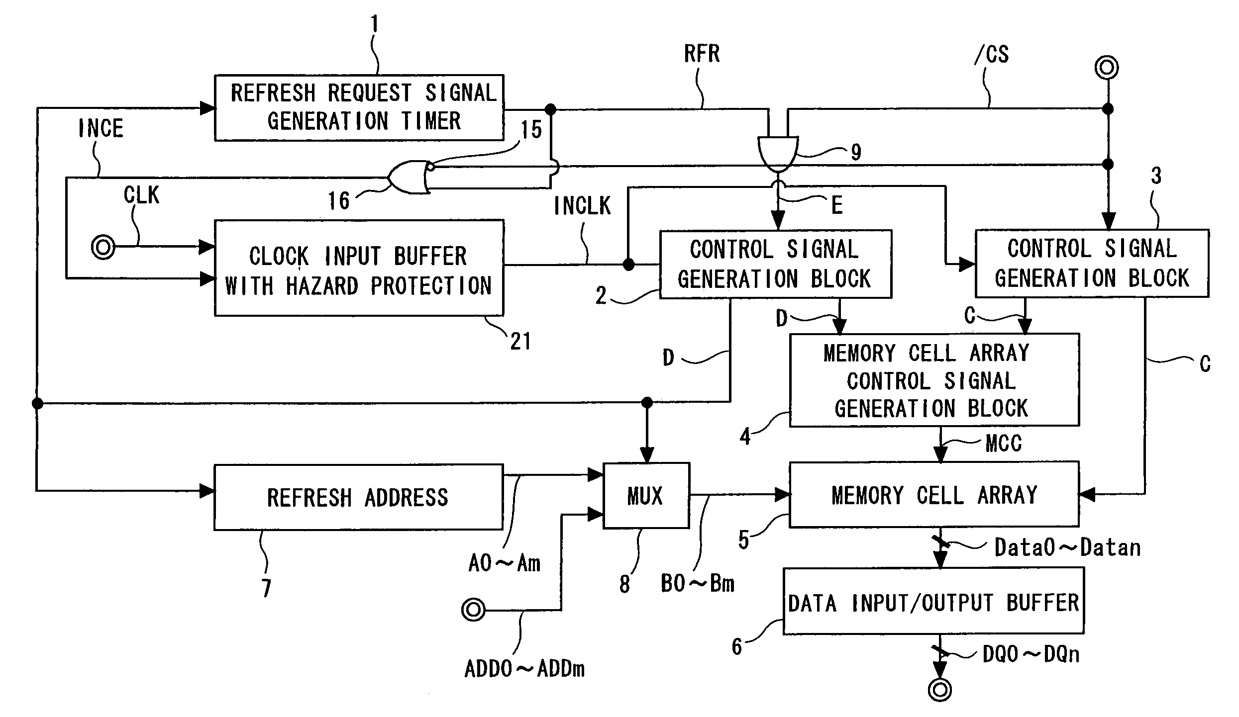
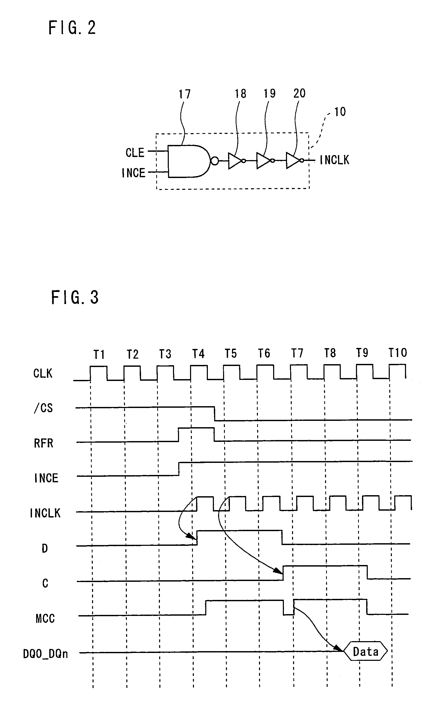
[0059]Preferred embodiments of the present invention are explained hereinafter in detail with reference to the accompanying drawings. Firstly, the present invention is explained below. FIG. 1 is a block diagram showing a semiconductor storage device according to this embodiment. FIG. 2 is a circuit diagram showing a clock input buffer 10 shown in FIG. 1. FIG. 3 is a timing chart when performing a read operation after a refresh operation in the semiconductor storage device according to this embodiment. FIG. 4 is a timing chart showing the operation between successive refresh operations in the semiconductor storage device according to this embodiment. In FIG. 1, the same elements as in FIGS. 15 and 17 are denoted by the same reference symbols and redundant description is omitted.
[0060]The semiconductor storage device of FIG. 1 is different from the conventional synchronized semiconductor storage device of FIG. 17 in the part enclosed by a frame 14. This semiconductor storage device ha...
second embodiment
[0077]Now, the operation of the semiconductor storage device having the above structure is explained below. Referring to FIGS. 7 and 8, the Q output of the D flip-flop 33 is High in the initial state. In this state, a clock signal CLK from outside and an internal clock enable signal INCE from the OR circuit 16 are input to the clock input buffer 21 with hazard protection.
[0078]The operation when the internal clock enable signal INCE is High is as follows. Since High level of internal clock enable signal INCE is input, the output of the inverter 24 is Low. If the clock signal CLK is Low, the output of the NOR circuit 23 is High to set the Reset-Set flip-flop 25. The N transistor 28 thereby turns on, and the input of the inverter 26 is Low and the output of the inverter 26 is High. Thus, the output of the inerter 30 is Low, and the output of the NAND circuit 31 is High. The output of the NAND circuit 22 is thereby High, and the internal clock signal INCLK is Low.
[0079]Even if the clo...
fourth embodiment
[0088]Finally, the present invention is explained hereinafter. FIG. 13 is a block diagram showing a semiconductor storage device according to this embodiment. FIG. 14 is a circuit diagram showing a clock input unit shown in FIG. 13. As shown in FIGS. 13 and 14, this embodiment applies the present invention to the conventional semiconductor storage device described in Japanese Unexamined Patent Application Publication 2002-184180 explained earlier, providing a self refresh SDRAM. This embodiment replaces the clock input buffer in this conventional semiconductor storage device with a clock input unit 41, and places the refresh request signal generation timer 1 between a command decoder and a command latch. The refresh request signal generation timer 1 is activated by the input of a self refresh entry signal SRE and automatically outputs a refresh request signal RFR at a constant period. The clock input unit 41 receives the self refresh entry signal SRE and the refresh request signal R...
PUM
 Abstract
Description
Claims
Application Information
 - R&D
- Intellectual Property
- Life Sciences
- Materials
- Tech Scout
- Unparalleled Data Quality
- Higher Quality Content
- 60% Fewer Hallucinations
Browse by: Latest US Patents, China's latest patents, Technical Efficacy Thesaurus, Application Domain, Technology Topic, Popular Technical Reports.
© 2025 PatSnap. All rights reserved.Legal|Privacy policy|Modern Slavery Act Transparency Statement|Sitemap|About US| Contact US: help@patsnap.com