End point detection for sputtering and resputtering

a technology of end point detection and sputtering, applied in the field of sputtering and resputtering, can solve the problems of introducing reliability problems, disadvantageous wide distribution, and difficult reflow ou

Inactive Publication Date: 2006-05-23
APPLIED MATERIALS INC
View PDF17 Cites 71 Cited by
  • Summary
  • Abstract
  • Description
  • Claims
  • Application Information

AI Technical Summary

Benefits of technology

[0018]In some applications, the chamber shield may be positioned to inhibit the deposition of conductor material or other opaque sputtered material onto the window, thereby permitting the deposition of material onto the substrate in a prior step or at the same time that material is being resputtered or etched from the substrate. Although deposition material may be deposited onto portions of the folded radiation path, in many applications, the deposition material will be sufficiently reflective to permit the emission spectra to be detected by a spectrometer or other suitable detector without significant signal loss. The etching or resputtering may be terminated when the detector detects that an underlying layer has been reached or when some other suitable process point has been reached.
[0019]The end point detection systems and methods of the present inventions may be used in a variety of chambers including sputtering chambers. One embodiment of the present inventions is directed to sputter depositing a liner material, such as tantalum or tantalum nitride, by combining long-throw sputtering, self-ionized plasma (SIP) sputtering, inductively-coupled plasma (ICP) resputtering, and coil sputtering in one chamber. Long-throw sputtering is characterized by a relatively high ratio of the target-to-substrate distance and the substrate diameter. SIP, particularly at low pressures (for example, below 5 mTorr), tends to be promoted by magnetrons having relatively small areas to thereby increase the target power density, and by magnetrons having asymmetric magnets causing the magnetic field to penetrate farther toward the substrate. Long-throw SIP sputtering promotes deep hole coating of both the ionized and neutral deposition material components.
[0020]ICP resputtering can reduce the thickness of layer bottom coverage of deep holes to reduce contact resistance. During ICP resputtering, ICP coil sputtering can deposit a protective layer, particularly on areas such as adjacent the hole openings where thinning by resputtering may not be desired. During the ICP resputtering, the emissions of the plasma may be monitored through a folded radiation path to a detector positioned either outside a chamber window or within the chamber pressure walls but protected from sputter deposition by a suitable shield. Once the appropriate emissions have been detected, the ICP resputtering may be terminated.

Problems solved by technology

Lining and filling via holes and similar high aspect-ratio structures, such as occur in dual damascene, have presented a continuing challenge as their aspect ratios continue to increase.
Such a wide distribution can be disadvantageous for filling a deep and narrow via hole 122 such as that illustrated in FIG. 2, in which a barrier layer 124 has already been deposited.
Once a void 134 has formed, it is often difficult to reflow it out by heating the metallization to near its melting point.
Even a small void can introduce reliability problems.
If a second metallization deposition step is planned, such as by electroplating, the bridged overhang makes subsequent deposition more difficult.

Method used


Image

  • End point detection for sputtering and resputtering
  • End point detection for sputtering and resputtering
  • End point detection for sputtering and resputtering

Examples


Embodiment Construction

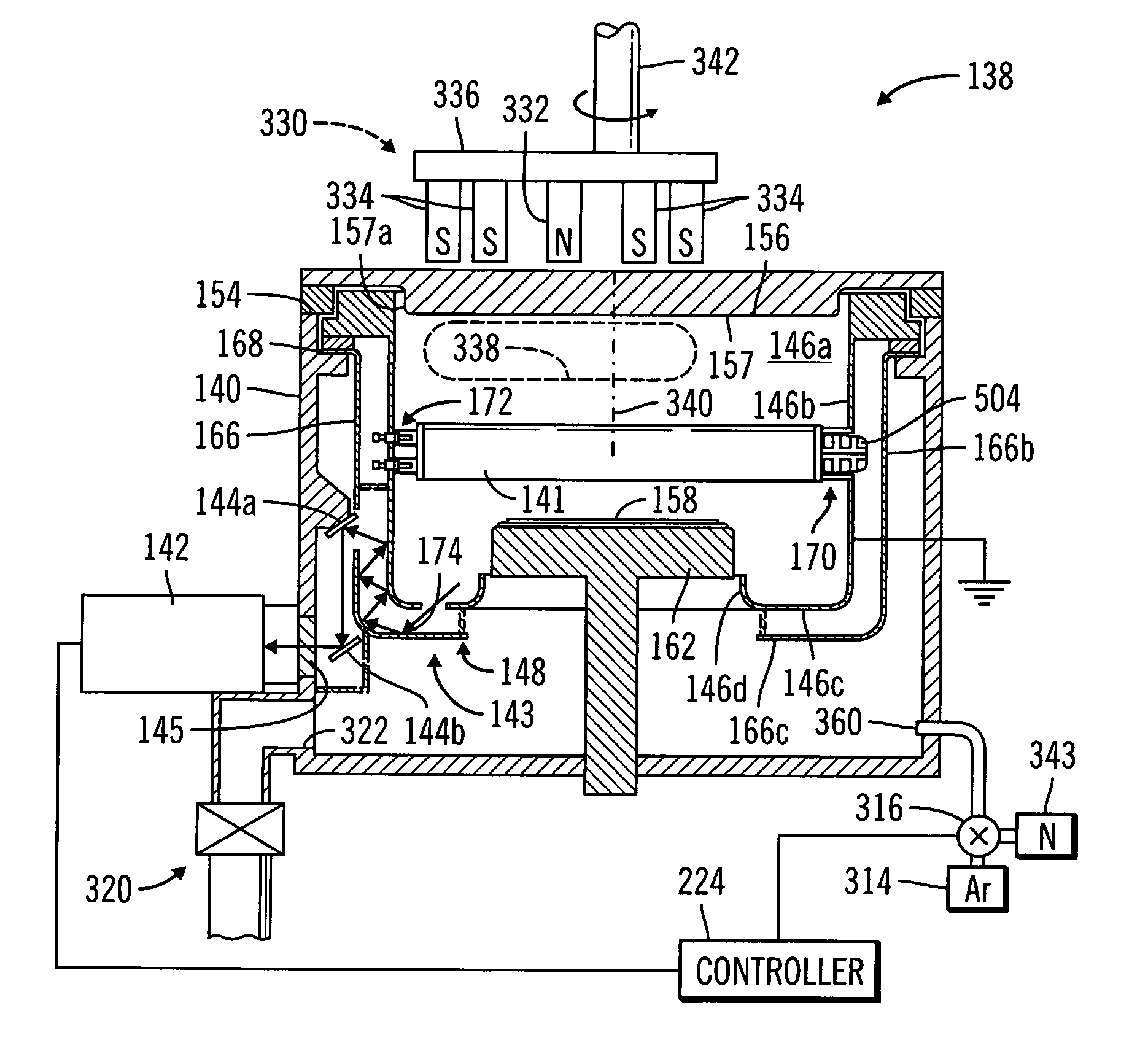
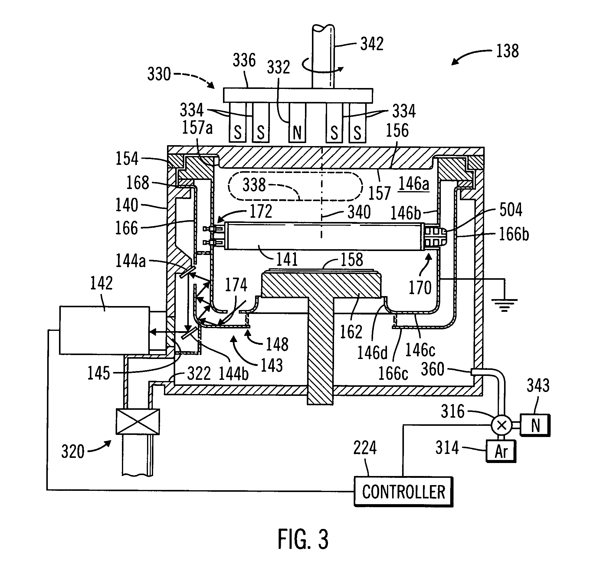
[0017]Plasma etching or resputtering of a layer of sputtered materials including opaque metal conductor materials may be controlled in a sputter reactor system. In one embodiment, resputtering of a sputter deposited layer is performed while additional material is being sputter deposited onto a substrate. A path positioned within a chamber of the system directs light or other radiation emitted by the plasma to a chamber window or other optical view-port which is protected by a shield against deposition by the conductor material. In one embodiment, the radiation path is folded to reflect plasma light around the chamber shield and through the window to a detector positioned outside the chamber window.

[0018]In some applications, the chamber shield may be positioned to inhibit the deposition of conductor material or other opaque sputtered material onto the window, thereby permitting the deposition of material onto the substrate in a prior step or at the same time that material is being r...


PUM

PropertyMeasurementUnit
widthsaaaaaaaaaa
thicknessaaaaaaaaaa
sizesaaaaaaaaaa

Abstract

Plasma etching or resputtering of a layer of sputtered materials including opaque metal conductor materials may be controlled in a sputter reactor system. In one embodiment, resputtering of a sputter deposited layer is performed after material has been sputtered deposited and while additional material is being sputter deposited onto a substrate. A path positioned within a chamber of the system directs light or other radiation emitted by the plasma to a chamber window or other optical view-port which is protected by a shield against deposition by the conductor material. In one embodiment, the radiation path is folded to reflect plasma light around the chamber shield and through the window to a detector positioned outside the chamber window. Although deposition material may be deposited onto portions of the folded radiation path, in many applications, the deposition material will be sufficiently reflective to permit the emission spectra to be detected by a spectrometer or other suitable detector without significant signal loss. The etching or resputtering may be terminated when the detector detects that an underlying layer has been reached or when some other suitable process point has been reached.

Description

RELATED APPLICATIONS[0001]This application claims the benefit of the U.S. Provisional Application No. 60 / 410,843 filed Sep. 13, 2002, which is incorporated by reference in entirety.FIELD OF THE INVENTION[0002]The inventions relate generally to sputtering and resputtering. In particular, the inventions relate to the sputter deposition of material and resputtering of deposited material in the formation of semiconductor integrated circuits.BACKGROUND ART[0003]Semiconductor integrated circuits typically include multiple levels of metallization to provide electrical connections between large numbers of active semiconductor devices. Advanced integrated circuits, particularly those for microprocessors, may include five or more metallization levels. In the past, aluminum has been the favored metallization, but copper has been developed as a metallization for advanced integrated circuits.[0004]A typical metallization level is illustrated in the cross-sectional view of FIG. 1. A lower-level l...

Claims


Application Information

Patent Timeline
Patent Type & Authority Patents(United States)
IPC IPC(8): C23C14/35C23C14/04C23C14/16C23C14/32C23C14/54C23C14/58G01N21/68H01J37/32H01L21/285H01L21/66H01L21/768
CPCC23C14/046C23C14/165C23C14/544C23C14/5833C23C14/5873G01N21/68H01J37/321H01J37/32477H01J37/32935H01J37/32963H01J37/3455H01L21/2855H01L21/76814H01L21/76844H01L21/76846H01L21/76862H01L21/76865H01L22/26H01L2924/0002H01L2924/00
Inventor SOMEKH, SASSON R.SCHWEITZER, MARC O.FORSTER, JOHN C.XU, ZHENGMOSELY, RODERICK C.CHIN, BARRY L.GRUNES, HOWARD E.
Owner APPLIED MATERIALS INC
Why Eureka
Try Eureka