Integrated optical multiplexer and demultiplexer for wavelength division transmission of information

a wavelength division and information technology, applied in the field of wavelength division optical transmission of information, can solve the problems of increasing the delay of interconnection, the large size and bulkiness of optical multiplexers such as those disclosed in the above patents, and the rapid development of interconnections formed of conventional electrical interconnections and switching technology, so as to achieve faster data throughput and high-intensity optical signals.

Inactive Publication Date: 2006-05-23
ADVANCED INTERFACES GEORGIA
View PDF46 Cites 80 Cited by
  • Summary
  • Abstract
  • Description
  • Claims
  • Application Information

AI Technical Summary

Benefits of technology

[0022]Since optics is reversible, the invention also contemplates an optical multiplexer for multiplexing discrete wavelength light beams modulated with data into a wavelength division multiplexed optical signal for transmission. In the multiplexer, the photo detectors are replaced with photo emitters for emitting the discrete wavelength light beams and the conditioning electronics functions to reformat data to be transmitted and modulate the data onto light beams emitted by the emitters. Thus, an on-chip micro- or nano-scale optical interconnection network for microelectronic chips is now possible through application of the present invention. The binary blazed grating of the invention can be fabricated on these scales in...

Problems solved by technology

The size of such devices generally is not an issue in the telecommunications industry and, thus, optical multiplexers and demultiplexers such as those disclosed in the above patents and others tend to be relatively large and bulky.
As integrated circuit feature sizes continue to decrease and chip sizes continue to increase, interconnections formed of conventional electrical interconnects and switching technology are rapidly becoming a critical issue in the realization of microelectronic systems.
The interconnection delay can even increase if chip size is scaled up.
At some point in this scaling process, interconnection delay will dominate system speed; i.e., system speed will not be able to track increasing device speed performance due to the interconnection delay.
Conventional conductor and semiconductor interconnects are not able to sustain the required future data rates of 40 Gb/s or higher.
Thus conventional interconnects between features on future chips will be an insurmountable bottleneck to the throughput of high-density data communication systems and will be unworkable in future high-speed microelectronics.
There are two major challenges to the introduction of optical interconnections to microelectronic data communication systems such as computer chips.
Second, optical component technology on a micro- or nano-optical scale necessary for implementation of on-chip optical interconnects is not mature and it is costly.
Further, due to power and heat dissipation constraints present in a microelectronic circuit environment, these micro-optical multiplexers and demultiplexers must operate with virtually no optical transmission losses, otherwise the data throughput will be compromised.
When an incident beam is a multiplexed polychromatic beam, each discrete wavelength component beam within the incident beam is diffracted at a different angle and thus the component beams are fanned out and separated, resulting in demultiplexi...

Method used


Image

  • Integrated optical multiplexer and demultiplexer for wavelength division transmission of information
  • Integrated optical multiplexer and demultiplexer for wavelength division transmission of information
  • Integrated optical multiplexer and demultiplexer for wavelength division transmission of information

Examples


Embodiment Construction

[0031]The following description of the present invention is provided as an enabling teaching of the invention in its best, currently known embodiment. Those skilled in the relevant art will recognize that changes can be made to the embodiments described, while still obtaining the beneficial results of the present invention. Accordingly, those who work in the art will recognize that modifications and adaptations to the present invention are possible and may even be desirable in certain circumstances, and are a part of the present invention. Thus, the following description is provided as illustrative of the principles of the present invention and not in limitation thereof since the scope of the present invention is defined by the claims.

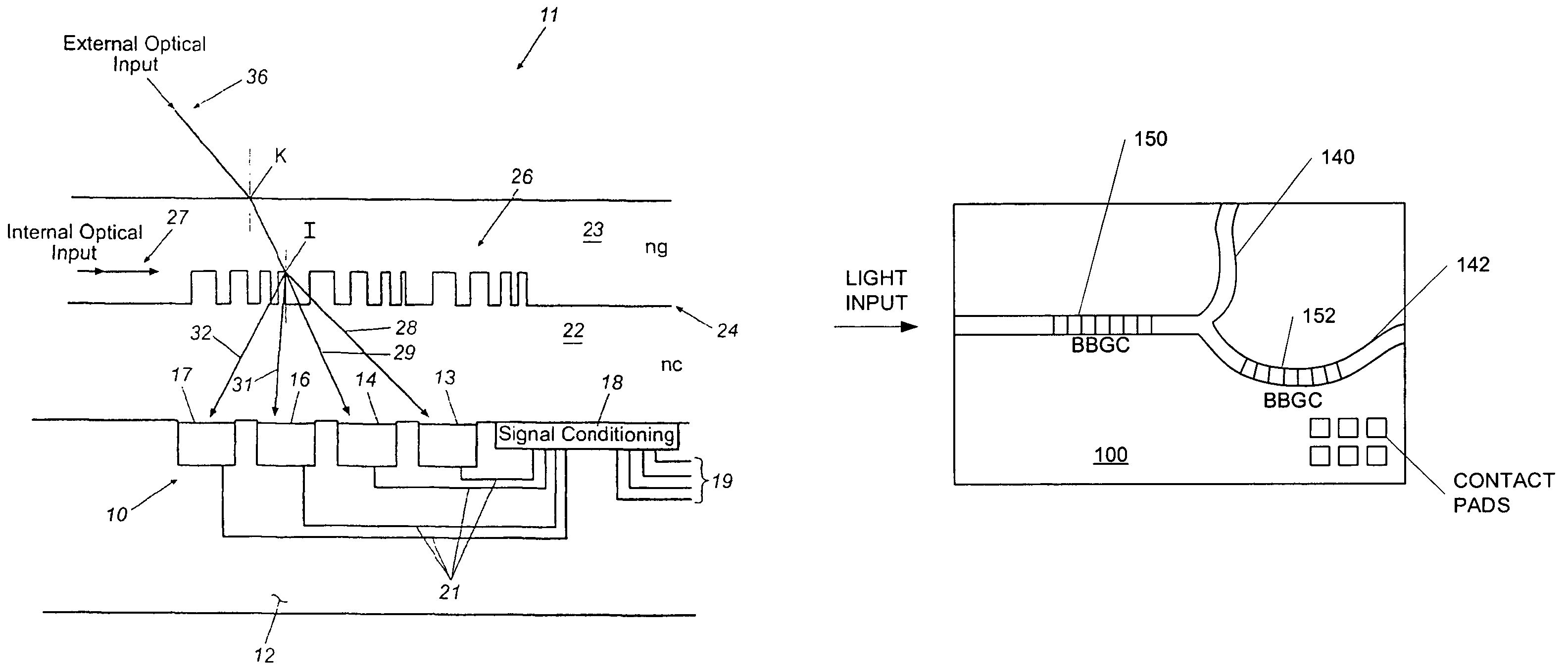
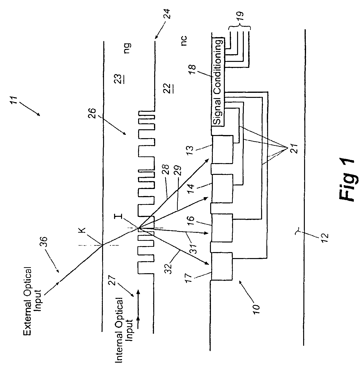
[0032]Referring now in more detail to the drawing, FIG. 1 illustrates an integrated optical demultiplexer that embodies principles of the invention in a preferred form. It will be understood that the figure includes only the very small section of a mic...


PUM


Abstract

A multiplexer/demultiplexer is provided for optical interconnection between electronic components on an integrated circuit chip. The multiplexer/demultiplexer includes a substrate formed with an array of photo emitters/detectors and conditioning electronics coupled thereto. A first layer of optically transparent material is formed on the substrate overlying the emitters/detectors and a second layer of optically transparent material, functioning as an optical waveguide, is formed on the first layer. A binary blazed grating is formed at the interface of the two layers. For multiplexing, discrete wavelength optical signals are modulated with data, emitted by the emitters, intercepted by the binary blazed grating, and multiplexed into a polychromatic beam for transmission through the waveguide. For demultiplexing, the discrete wavelengths are separated by the binary blazed grating and directed to corresponding detectors. The conditioning electronics receive and demodulate the output of the detectors to extract data, and format the data for communication with electronic components.

Description

CROSS REFERENCE TO RELATED APPLICATIONS[0001]This is a continuation-in-part of application Ser. No. 10 / 281,790, filed on Oct. 28, 2002, now U.S. Pat. No. 6,718,093, which is a continuation of application Ser. No. 09 / 722,989, filed on Nov. 27, 2000, now U.S. Pat. No. 6,490,393.FIELD OF THE INVENTION[0002]This invention relates generally to wavelength division optical transmission of information and more particularly to wavelength division optical multiplexers and demultiplexers for use in optical transmission systems.BACKGROUND[0003]Wavelength division multiplexing (WDM) is a valuable technique for increasing the information carrying capacity of optical transmissions for voice communications as well as high density transmission of data. In essence, WDM involves modulating light beams of multiple discrete wavelengths with information to be transmitted, combining or multiplexing the beams into a single polychromatic light beam, and transmitting the polychromatic beam to a receiving loc...

Claims


Application Information

Patent Timeline
IPC IPC(8): G02B6/34G01J3/02G01J3/18G02B5/18G02B6/12G02B6/124G02B6/43H01L27/144H01L31/105H01L31/12H01L31/18H04J14/02
CPCG01J3/02G01J3/18G02B5/1809G02B6/12002G02B6/12004G02B6/12007G02B6/124G02B6/43H01L27/1443H01L31/1804G01J3/0259Y02E10/547G02B2006/12107G02B2006/12173G02B2006/12176H01L31/105H01L31/12H01S5/0268H04J14/02Y02P70/50
Inventor ZHOU, ZHIPING JAMES
Owner ADVANCED INTERFACES GEORGIA
Why Eureka
Try Eureka