Semiconductor circuit designing method, semiconductor circuit designing apparatus, program, and semiconductor device

a semiconductor and circuit design technology, applied in the field of semiconductor circuit designing and semiconductor devices, can solve the problems of difficult calculation of the influence of crosstalk noise between the internal wiring b>1202/b> and the external wiring b>1203/b>, and the design of the entire semiconductor circuit on the flat layout is becoming difficult, so as to achieve simple, quick and accurate design of the semiconductor circuit.

Inactive Publication Date: 2006-05-23
SOCIONEXT INC
View PDF13 Cites 9 Cited by
  • Summary
  • Abstract
  • Description
  • Claims
  • Application Information

AI Technical Summary

Benefits of technology

[0028]Since the boundary part of the block can be shielded, an internal side and an external side of the boundary can be completely separated from each other so that the block can be considered as one independent part. This enables the lower level hierarchical designing and the upper level hierarchical designing to be independent from each other, thereby realizing simple, quick, and accurate designing of a semiconductor circuit.

Problems solved by technology

In accordance with an enhancement in integration and an increase in scale of an LSI (Large Scale Integration), flat layout designing of collectively processing the entire semiconductor circuit is becoming difficult.
Moreover, the calculation of the influence of a crosstalk noise between the internal wiring 1202 and the external wiring 1203 is also difficult.
In this case, too, the calculation of the wiring capacitance 1312 is difficult.
However, the following problems arise in accordance with miniaturization of technology.
(1) an increase in regions which are not usable in arrangement and wiring processing
At this time, this verification is not accurate since the verification is performed assuming a certain state as the boundary conditions of the block.
When the verification result indicates that the crosstalk noise gives an adverse effect, a crosstalk noise error is outputted.
When the verification result indicates that the timing is not within a prescribed value range, a timing error is outputted.
(1) The wiring capacitance value cannot be determined accurately since the conditions of the block boundaries are not fixed until the arrangement and wiring of the inside of the blocks of the lower level of hierarchy are finished.
(2) The influence due to the wirings only passing over the blocks has to be determined after the layout of the upper level of hierarchy.
(3) Due to a trouble occurring in the block boundaries, the processing from Step S1409 sometimes has to be repeated after Step S1429 in FIG. 14 to correct the blocks of the lower level of hierarchy again and to perform the error check again on the upper level of hierarchy.

Method used


Image

  • Semiconductor circuit designing method, semiconductor circuit designing apparatus, program, and semiconductor device
  • Semiconductor circuit designing method, semiconductor circuit designing apparatus, program, and semiconductor device
  • Semiconductor circuit designing method, semiconductor circuit designing apparatus, program, and semiconductor device

Examples


Embodiment Construction

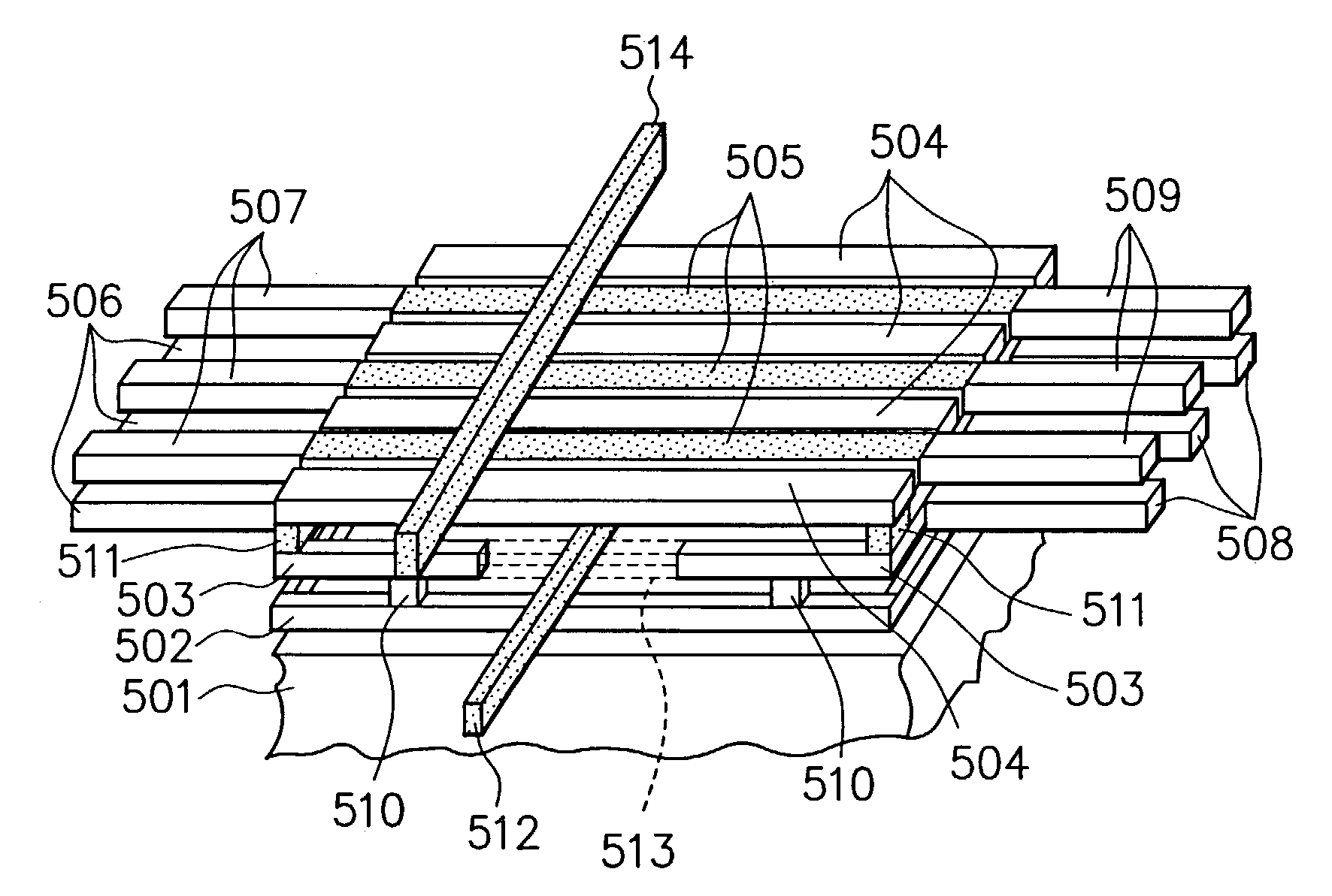
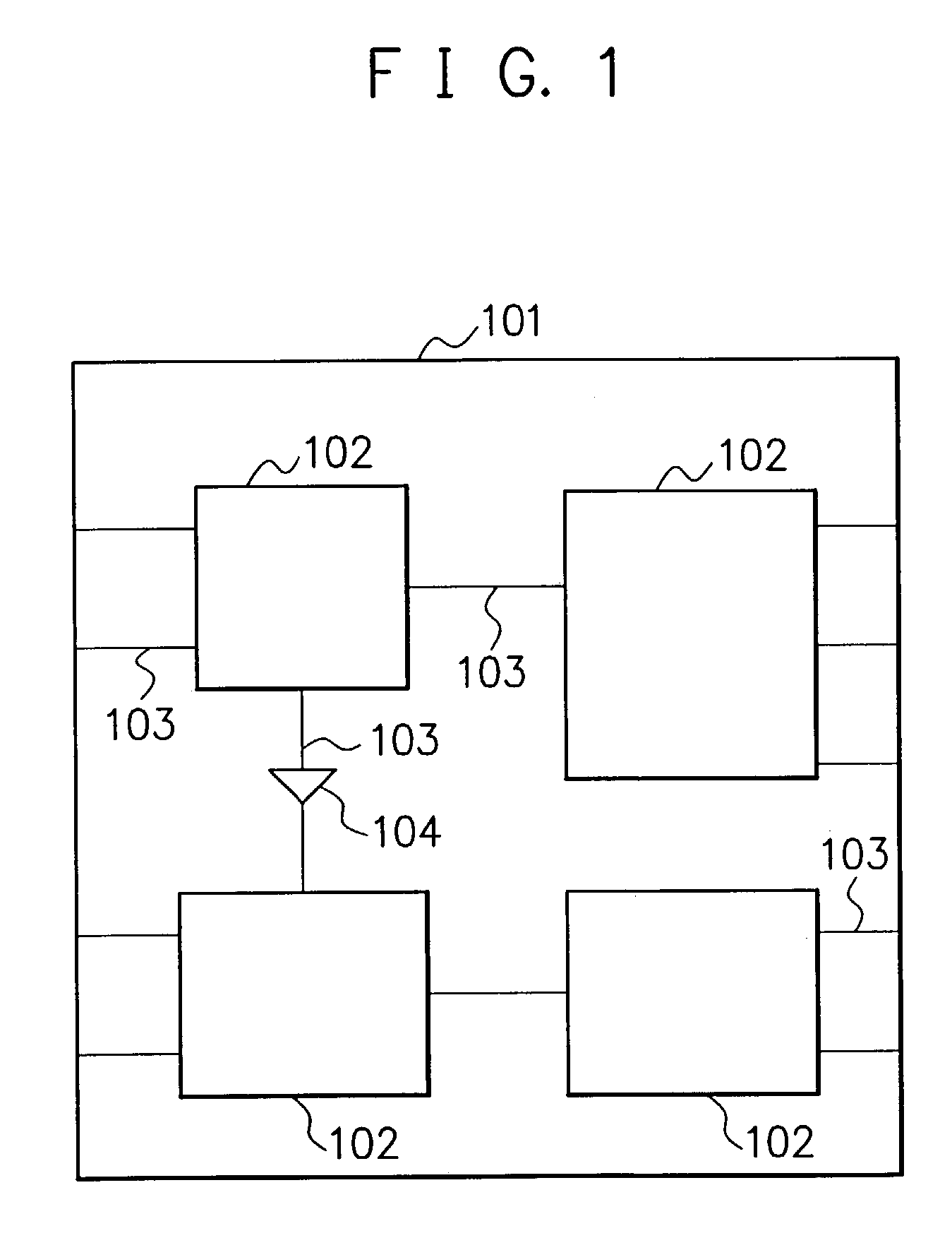
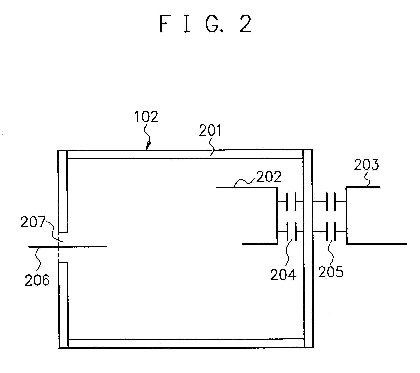
[0043]FIG. 1 is a plan view of a semiconductor circuit to be designed according to an embodiment of the present invention. A semiconductor chip 101 is a semiconductor device. A plurality of blocks 102 are provided on the semiconductor chip 101. The blocks 102 divide the semiconductor chip 101 according to the function, the number of gates, and the like. External wirings 103 are wirings in external parts of the blocks 102. A cell 104, which is a logical element, is provided in the external part of the block 102. Hierarchical designing is divided into upper level hierarchical designing and lower level hierarchical designing. In the lower level hierarchical designing, the arrangement, wiring, and so on of cells inside the block 102 are designed. In the upper level hierarchical designing, the arrangement of the cell 104, the layout of the external wirings 103, and so on are designed. Incidentally, hierarchical designing of three levels or more is also possible, providing an additional b...


PUM


Abstract

The present invention provides a semiconductor circuit designing method, comprising a lower level hierarchical designing step of designing a semiconductor circuit inside a block and an upper level hierarchical designing step of designing an external wiring of the block. The above-mentioned lower level hierarchical designing step or upper level hierarchical designing step includes a shield wiring designing step of designing to provide a shield wiring on a boundary part of the block.

Description

CROSS-REFERENCE TO RELATED APPLICATIONS[0001]This application is based upon and claims the benefit of priority from the prior Japanese Patent Application No. 2002-180889, filed on Jun. 21, 2002, the entire contents of which are incorporated herein by reference.BACKGROUND OF THE INVENTION[0002]1. Field of the Invention[0003]The present invention relates to a semiconductor circuit designing technique and a semiconductor device.[0004]2. Description of the Related Art[0005]In accordance with an enhancement in integration and an increase in scale of an LSI (Large Scale Integration), flat layout designing of collectively processing the entire semiconductor circuit is becoming difficult. Because of this, such a designing method has been applied that blocks are made on a lower level of hierarchy by dividing the inside of an LSI according to the function or the like, and the layout is designed for each of the blocks. This hierarchical layout has realized processing of large-scale data, where...

Claims


Application Information

Patent Timeline
Patent Type & Authority Patents(United States)
IPC IPC(8): G06F17/50H01L29/00H01L21/82H01L21/822H01L23/522H01L27/04
CPCG06F17/5077H01L23/5225H01L2924/0002H01L2924/00G06F30/394
Inventor TOMITA, KATSUKOSUGIOKA, TOSHIAKIBABA, KATSUTOSHI
Owner SOCIONEXT INC
Why Eureka
Try Eureka