Junction structure and junction method for conductive projection

a junction structure and conductive projection technology, applied in the direction of resist details, electrical apparatus construction details, semiconductor/solid-state device details, etc., can solve the problems of reducing junction strength, affecting the strength of junctions, and affecting the reliability of junctions, so as to prevent the conductive projection from suffering mispositioning or aggregation, improve the strength and reliability of the junction portion, and reduce the amount of resin materials supplied

Inactive Publication Date: 2006-05-30
SONY CORP
View PDF5 Cites 8 Cited by
  • Summary
  • Abstract
  • Description
  • Claims
  • Application Information

AI Technical Summary

Benefits of technology

[0011]As a method for avoiding the warpage, there is a method in which the reinforcing resin material is supplied by a screen printing process only to the conductor portion to which the conductive projection is joined, but this method has a problem in that printing is difficult when the pitches between the conductive projections are narrower.
[0025]By the present invention, the conductive projection is joined to the surface of the conductor portion which is formed at the same level as that of the surface of the insulating layer so that the root portion of the conductive projection is surrounded by the resin material in a ring form. Therefore, even when the amount of the resin material supplied is reduced for suppressing warpage, a fillet having a large height can be obtained to improve the junction portion in strength and reliability, as compared to that in a structure without planarization. Accordingly, high wiring density can be achieved by reducing the size of the conductive projection without increasing the number of layers of interconnection to cause the substrate to have a large thickness.

Problems solved by technology

For this reason, when applying the reinforcing resin material to the root portion of the conductive projection, the resin material is disadvantageously supplied along the steps, so that the amount of the resin material supplied is not uniform and a fillet 46 at a certain position cannot have a satisfactory height, leading to a disadvantage in that the junction strength may be lowered.
When the amount of the resin material supplied is increased for obtaining a desired fillet height or preventing the fillet from having an ununiform height, shrinkage on curing of the increased resin material causes strain in the interposer, so that a problem in that the semiconductor package suffers warpage is likely to occur.
As a method for avoiding the warpage, there is a method in which the reinforcing resin material is supplied by a screen printing process only to the conductor portion to which the conductive projection is joined, but this method has a problem in that printing is difficult when the pitches between the conductive projections are narrower.

Method used


Image

  • Junction structure and junction method for conductive projection
  • Junction structure and junction method for conductive projection
  • Junction structure and junction method for conductive projection

Examples


first embodiment

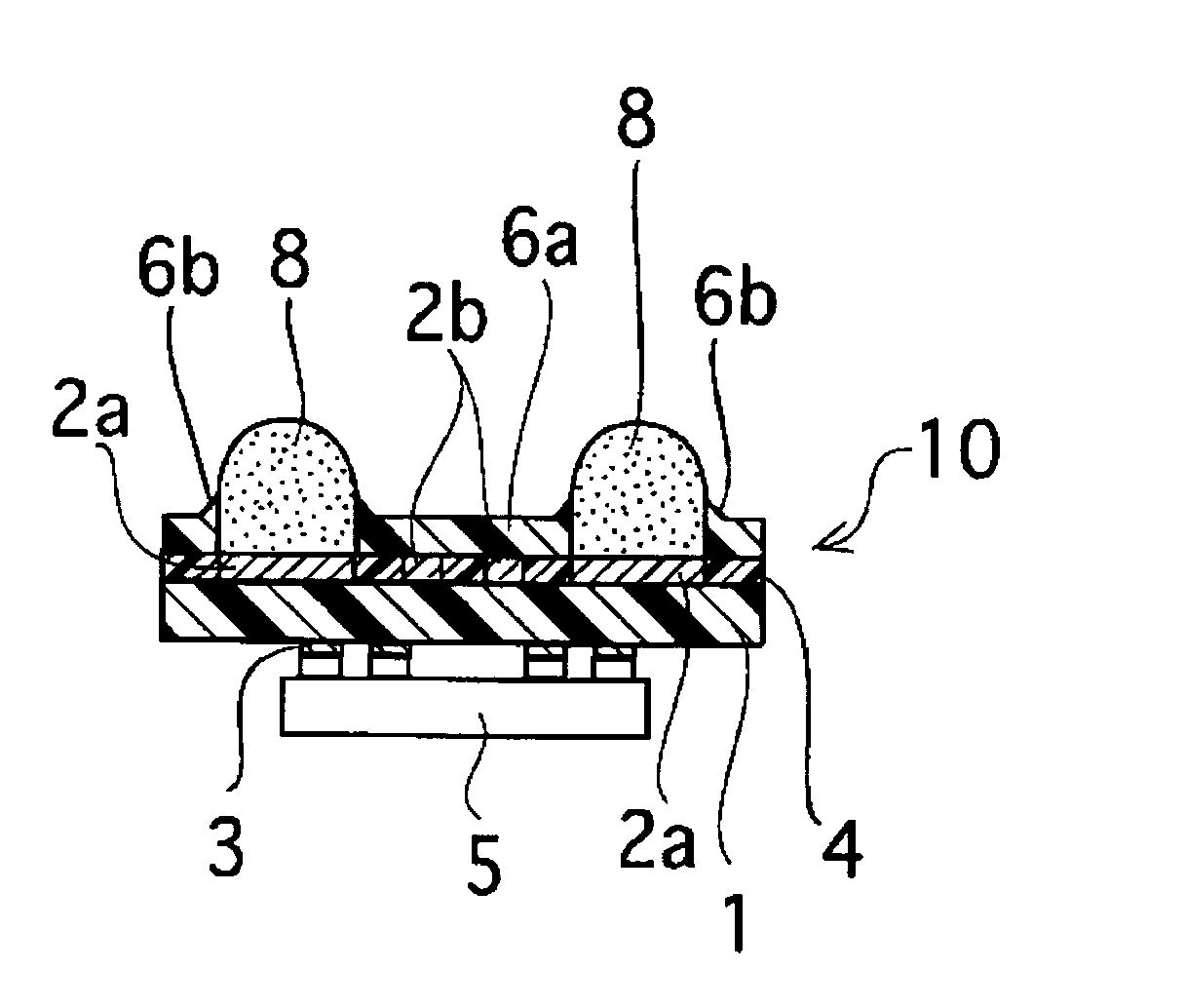
[0043]In the present embodiment, as one example of the junction structure and junction method of the present invention, a structure in which a conductive projection is joined to an interposer, on which conductor portions (wiring and land) are formed for rearrangement of electrode portions of a semiconductor bare chip to be mounted is formed to a larger pitch, so that a root portion of the conductive projection is reinforced by a resin, and a junction method for the structure will be described. FIGS. 1 to 4 illustrate process steps for the junction.

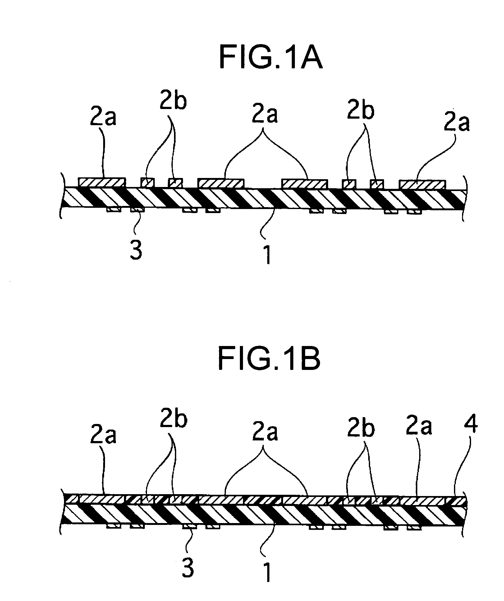
Process Step of FIG. 1A

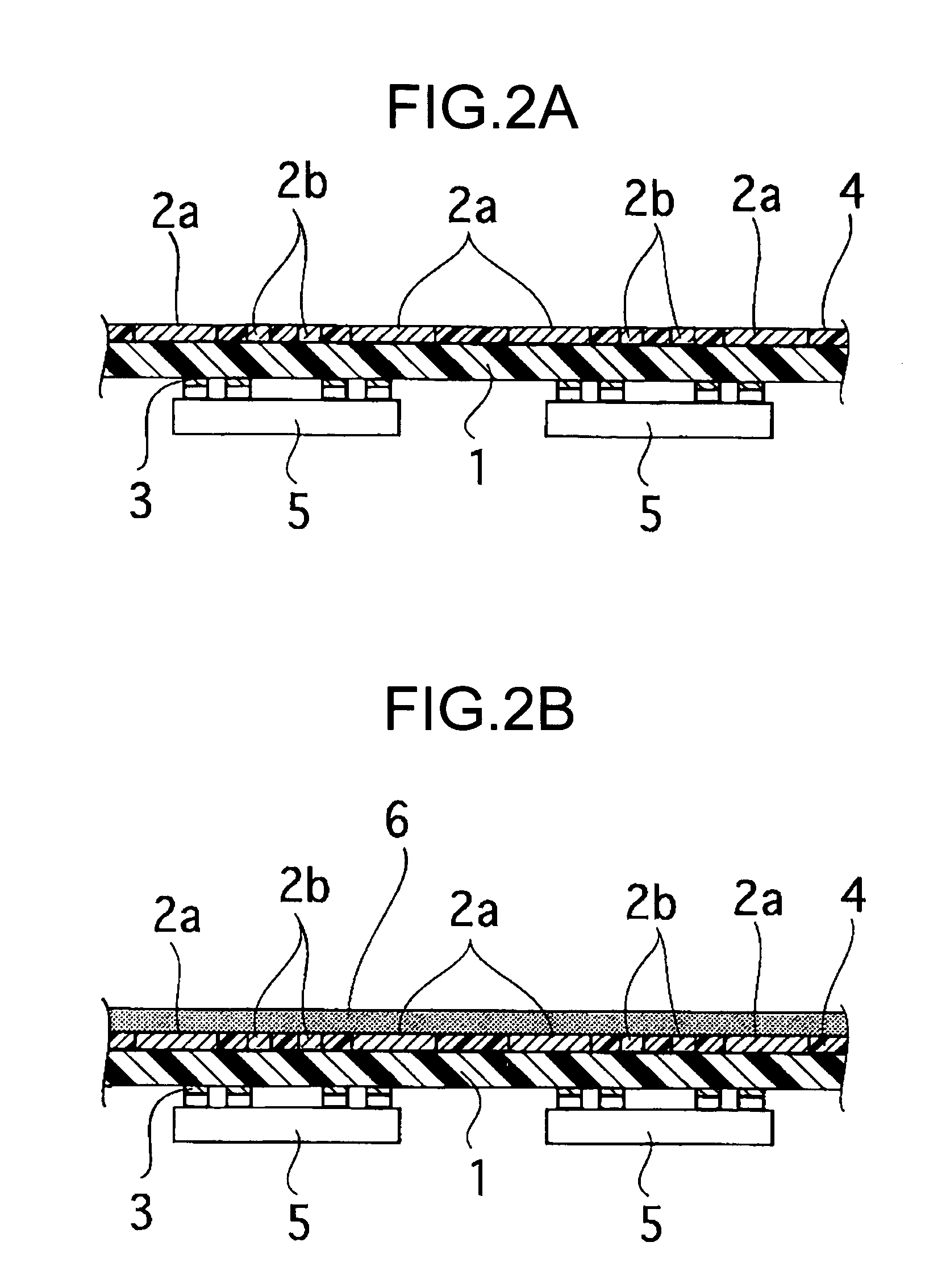
[0044]First, a substrate including an insulating layer 1 having formed on both surfaces thereof conductor portions 2a, 2b, 3 is prepared or provided. For example, the conductor portions 2a, 2b, 3 are formed in a desired pattern on the insulating layer 1 by a subtractive method in which a flat metal foil is bonded onto the insulating layer 1 and then an unnecessary portion of the metal foil is etched, or an additive m...

second embodiment

[0068]Next, the second embodiment of the present invention will be described. In the first and second embodiments, like constituent parts or portions are indicated by like reference numerals, and the overlapping detailed description is omitted.

[0069]In the first embodiment, as the resin material 6 for reinforcing the junction portion, an ultraviolet-curing resin material is mentioned as an example, but, when forming the fillet 6b around the root portion of the conductive projection 8, the resin material does not necessarily have ultraviolet curing properties.

[0070]In this case, the resin material 6 does not serve as a solder resist for protecting the conductor portion 2b and hence, as shown in FIG. 7A, there is a need to form a solder resist 9 for covering the conductor portion 2b on the surface of the insulating layer 4 which has preliminarily been subjected to planarization.

[0071]Then, as shown in FIG. 7B, the resin material 6 in a paste state is supplied by a printing process onl...

example 1

STRUCTURE OF EXAMPLE 1

[0075]FIG. 5 is a perspective view of an essential portion of a substrate for evaluation in Example 1. A printed wiring board including a base material 14 having a 30 mm×30 mm size, having 12 points of copper lands (conductor portions) 12 each having a diameter of 300 μm, and having 12 points of copper lands (conductor portions) 12 each having a diameter of 200 μm was prepared, and this printed wiring board was used as a substrate for evaluation. As the base material, glass fiber impregnated with an epoxy resin (grade FR-4) was polished. The base material has a thickness of 0.4 mm, and each conductor portion 12 has a thickness of 18 μm.

[0076]An insulating layer 14 comprised of an epoxy resin was applied to the evaluation substrate so that the thickness of the layer became 20 μm, and cured to cover the conductor portions 12 and fill portions between the conductor portions 12. Subsequently, the cured insulating layer 14 was abraded so that the surfaces of the con...


PUM

PropertyMeasurementUnit
diameteraaaaaaaaaa
diameteraaaaaaaaaa
sizeaaaaaaaaaa

Abstract

To provide a junction structure and a junction method for conductive projection advantageous in that a required reinforcement strength can be obtained while suppressing the amount of a reinforcing resin material supplied to prevent warpage due to curing shrinkage. A conductive projection is joined to the surface of a conductor portion formed at the same level as that of the surface of the insulating layer so that a root portion of the projection is surrounded by a fillet-form resin material. The resin material contains an activator which assists in the junction between the conductive projection and the conductor portion when the resin material is in an uncured state, and is fused by heating to wet and rise the root portion of the conductive projection so as to be in a fillet form. The resin material is cured by an ultraviolet light while excluding the resin material on the conductor portion.

Description

CROSS REFERENCE TO RELATED APPLICATIONS[0001]The present document is based on Japanese Priority Document JP2003-077343, filed in the Japanese Patent Office on Mar. 20, 2003, the entire contents of which being incorporated herein by reference.BACKGROUND OF THE INVENTION[0002]1. Field of the Invention[0003]The present invention relates to a junction structure and a junction method of conductive projection used for making electrical and mechanical connection when mounting, for example, semiconductor parts on a wiring board, such as a mother board. More particularly, the present invention is related to a junction structure of conductive projection, which is joined to a planarized surface having no steps by surrounding its root portion with a resin material in a ring form to have high junction strength, and to a junction method of the conductive projection.[0004]2. Description of Related Art[0005]In recent years, as electronic apparatuses are being further miniaturized and sophisticated,...

Claims


Application Information

Patent Timeline
Patent Type & Authority Patents(United States)
IPC IPC(8): H05K1/11H01R12/04H01L23/12H01L21/60H01L23/32H02G3/08H05K3/34
CPCH05K3/3452H05K3/3478H05K2201/10734H05K2201/10977Y10T29/49147H05K2203/043H05K2203/0594H01L2224/10126H05K2203/041H01L2224/16227H01L2224/97H01L2924/15311H01L2224/81H01L21/60
Inventor ORUI, KENJINNO, HIROKONISHITANI, YUJIASAMI, HIROSHI
Owner SONY CORP
Why Eureka
Try Eureka