Chip package structure

a technology of chip and package, applied in the direction of semiconductor devices, semiconductor/solid-state device details, electrical apparatus, etc., can solve the problems of unsuitable economic mass production methods, large heat dissipation problems of chip manufacturers, and large time consumption of chip bonding materials, etc., to achieve superior electrical performance and high heat dissipation capacity of the package

Active Publication Date: 2006-06-06
IND TECH RES INST +1
View PDF14 Cites 52 Cited by
  • Summary
  • Abstract
  • Description
  • Claims
  • Application Information

AI Technical Summary

Benefits of technology

[0013]Accordingly, one objective of the present invention is to provide a chip package structure that combines the superior electrical performance of a flip-chip bonded device with the high heat dissipating capacity of a package with a heat sink.
[0023]In brief, because a heat sink with an area larger than the chip is attached to the uppermost chip, the chip package has a fast heat-dissipating pathway. Hence, reliability of the chip package in computation is improved.

Problems solved by technology

However, as density of each package continues to increase, heat dissipation becomes a major problem facing chip manufacturers.
However, it takes considerable time to fill up the bonding gap between the chip 50 and the carrier 80 with liquid encapsulating material through capillary effect alone.
Hence, this method is unsuitable for economic mass production.
In other words, reliability of the package will be adversely affected.
However, the need to form an additional over mold layer 72 increases the overall processing time resulting a drop in productivity.
Although the simultaneous molding process is able to prevent delamination, the encapsulating material layer 74 covering the chip still leads to poor heat dissipation from the chip package structure 44.

Method used


Image

  • Chip package structure
  • Chip package structure
  • Chip package structure

Examples


example 1

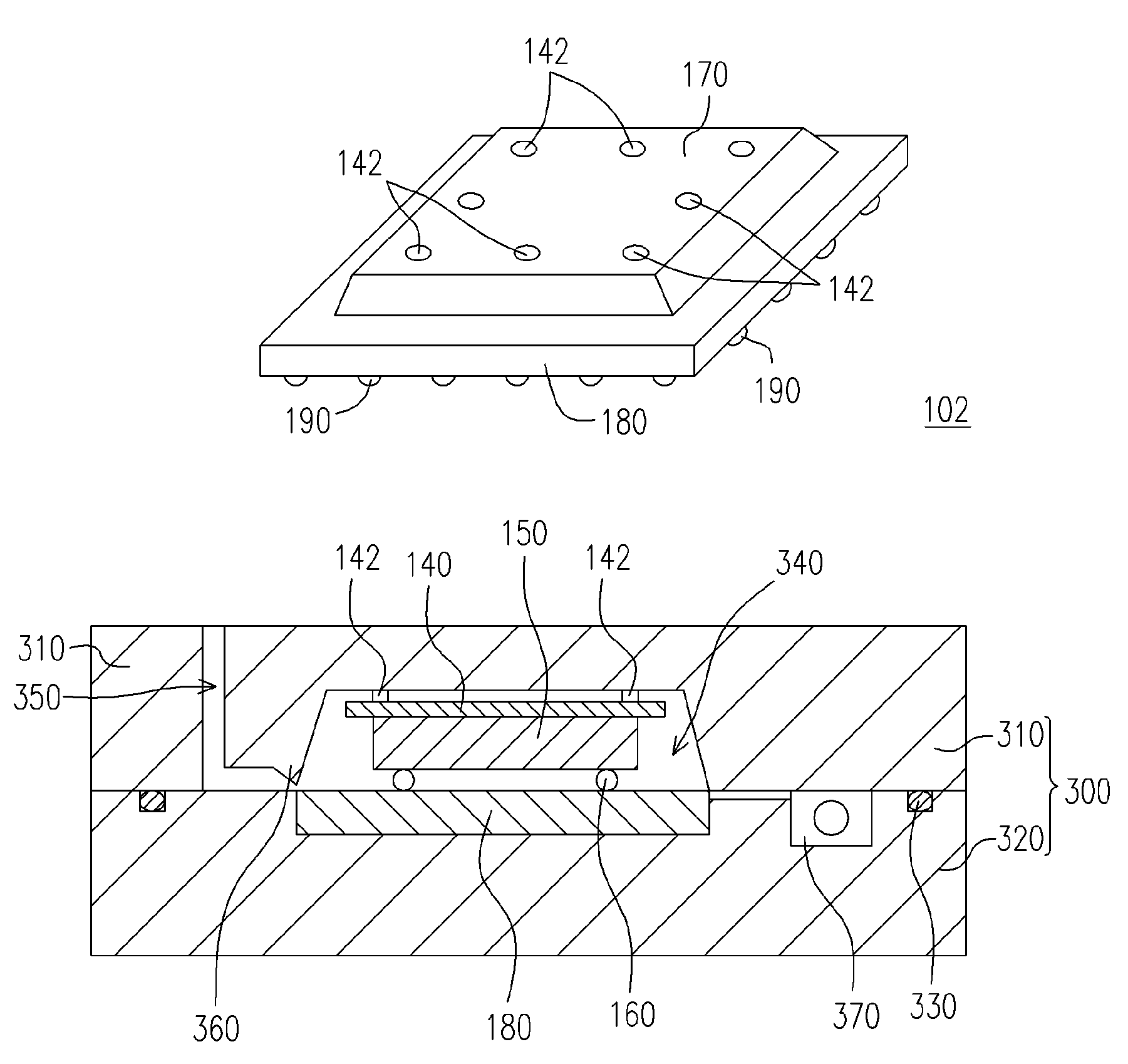
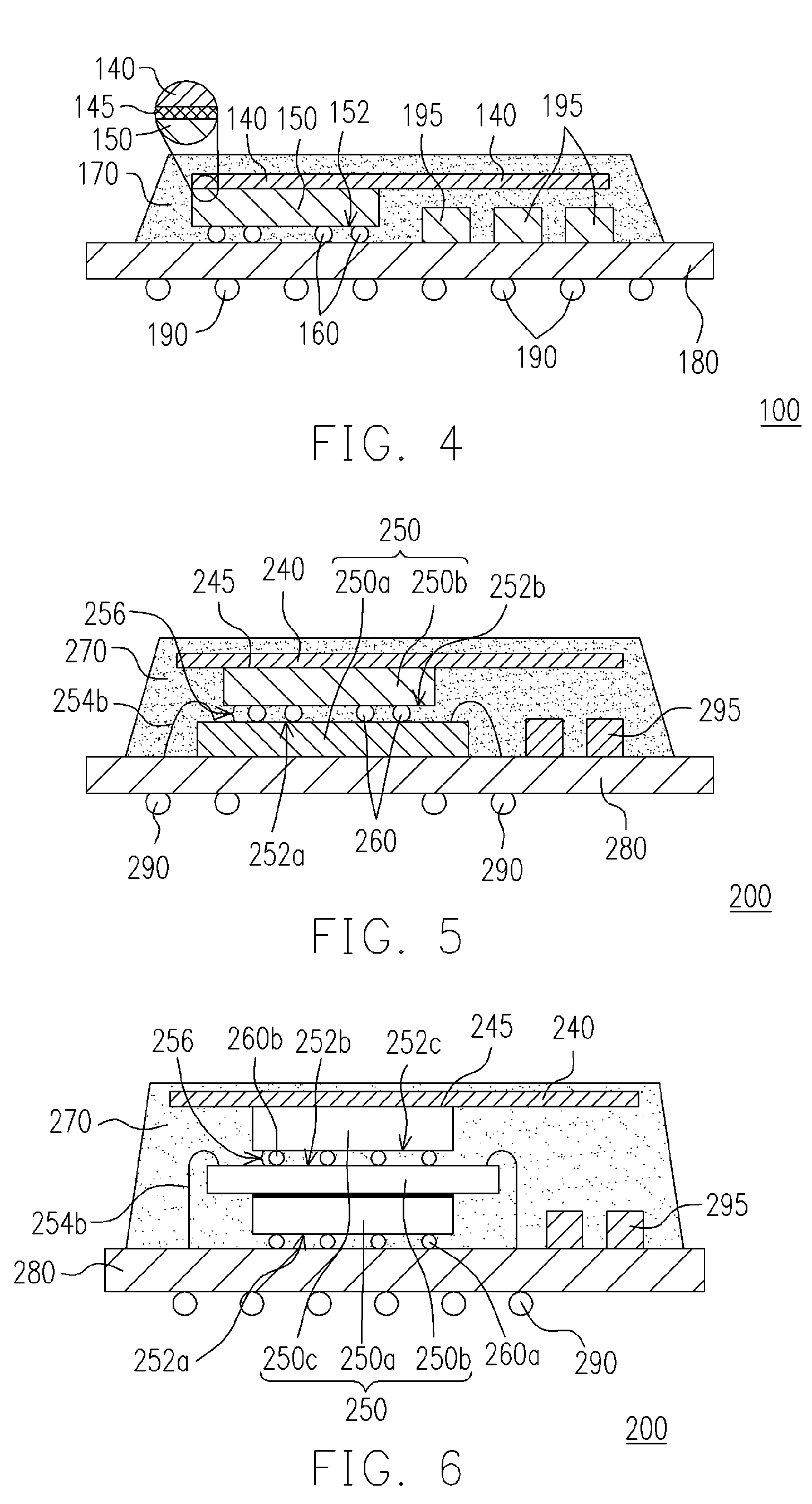
[0067]Chips each having a total area 8 mm×8 mm, 800 lead-tin bumps (melting point 183° C., pitch separation 0.25 mm) and a thickness 0.3 mm are set as an array over a FR-5 carrier with an area 35 mm×35 mm, a thickness 0.4 mm. To provide a uniform distribution of current, aluminum wires are set on the surface of the chip. The flip-chip bonding gap is between 50 to 75 μm. A 20 mm×20 mm heat sink with a thickness of about 0.15 mm is fabricated from a copper plate. The heat sink is attached to the carrier using a conventional thermal conductive adhesive material. To increase the bonding strength, the upper and lower surface of the copper heat sink is roughened. A set of transfer molding equipment with reduced-pressure molding capability is used for performing the reduced-pressure molding process. The pressure inside the mold cavity is reduced to an almost vacuum state of 1 mm-Hg during the molding process. The encapsulating material is comprised of CV8700F2 (having a maximum particle di...

example 2

[0068]Aside from changing the package thickness in example 1 to 0.6 mm, other aspects are the same so that a device as shown in FIG. 4 is formed. The thickness of the encapsulating material layer above the heat sink in a section through the device is between 0.08˜0.11 mm.

example 3

[0069]Aside from using a 0.2 mm aluminum plate to replace the 0.15 mm copper plate in example 1, other aspects are the same so that a device as shown in FIG. 4 is formed. The thickness of the encapsulating material layer above the heat sink in a section through the device is between 0.06˜0.10 mm.


PUM


Abstract

A chip package structure is disclosed. The chip package structure essentially comprises a carrier, one or more chips, a heat sink and an encapsulating material layer. At least one of the chips is bonded and electrically connected to the carrier or another chip using a flip-chip bonding technique. A flip-chip bonding gap is set up between the chip and he carrier or other chips. The heat sink is set up over the top chip. The heat sink has an area bigger than the chip. The encapsulating material layer fills up the flip-chip bonding gap and covers the carrier as well as the heat sink. The encapsulating material layer is formed in a simultaneous molding process and has a thermal conductivity more than 1.2 W / m.K. Furthermore, a plurality of standoff components may be selectively positioned on the heat sink.

Description

CROSS REFERENCE TO RELATED APPLICATIONS[0001]This application claims the priority benefit of Japan application serial no. 2003-117508, filed Apr. 22, 2003 and Taiwan application serial no. 92129521, filed Oct. 24, 2003.BACKGROUND OF INVENTION[0002]1. Field of the Invention[0003]The present invention relates to a chip package structure. More particularly, the present invention relates to a chip package structure with superior heat dissipating capacity.[0004]2. Description of the Related Art[0005]In this fast and ever-changing society, information matters to all people. Many types of portable electronic devices are produced which attempts to catch up with our desires to transmit and receive more data. Nowadays, manufacturers have to factor into their chip package many design concepts such as digital architecture, network organization, local area connection and personalized electronic devices. To do so demands special consideration in every aspects of the design process that affects th...

Claims


Application Information

Patent Timeline
Patent Type & Authority Patents(United States)
IPC IPC(8): H01L23/34H01L21/56H01L23/31H01L23/433H01L25/065
CPCH01L21/561H01L21/565H01L23/3128H01L23/4334H01L24/97H01L25/0657H01L24/45H01L2224/16145H01L2224/45124H01L2224/48091H01L2224/48227H01L2224/73253H01L2224/97H01L2225/0651H01L2225/06513H01L2225/06582H01L2225/06589H01L2924/01002H01L2924/01005H01L2924/01013H01L2924/01014H01L2924/01029H01L2924/01047H01L2924/0105H01L2924/01074H01L2924/01078H01L2924/01079H01L2924/01082H01L2924/15311H01L2924/19041H01L2924/19043H01L2924/19105H01L24/48H01L2924/01006H01L2924/01019H01L2924/01033H01L2924/01087H01L2924/01028H01L2224/16225H01L2224/32145H01L2224/32225H01L2224/73204H01L2224/73265H01L2924/00014H01L2224/81H01L2924/00H01L2224/48237H01L2924/15787H01L2924/181H01L2224/32245H01L2224/0401H01L2924/00012
Inventor CHEN, KAI-CHIHUANG, SHU-CHENLI, HSUN-TIENLEE, TZONG-MINGFUKUI, TARONEMOTO, TOMOAKI
Owner IND TECH RES INST
Why Eureka
Try Eureka