
Optoelectronic transceiver

Inactive Publication Date: 2006-06-06
DR JOHANNES HEIDENHAIN GMBH
View PDF23 Cites 15 Cited by
  • Summary
  • Abstract
  • Description
  • Claims
  • Application Information

AI Technical Summary

Benefits of technology

[0007]An advantage and object of the present invention is therefore to refine the optoelectronic transceiver for bidirectional data transmission by optical waveguides, as generically defined at the outset, in such a way that in particular still further-increased insensitivity with regard to the adjustment of the various elements relative to the optical waveguide and thus a reduced effort and expense of assembly results. Furthermore, the simplest possible production of such a device is desirable.
[0009]According to the present invention, it is now provided that at least the active radiation-sensitive layer region of the receiving unit be disposed perpendicular to the axis of the receiving unit, along which the receiving unit and the transmitting unit are disposed. This axis is preferably predetermined by the optical axis of symmetry of the optical waveguide. This arrangement becomes possible in particular by the use according to the present invention of special optoelectronic receiving units, in which the active layer region is located in a thin membrane through which light can be projected by the transmitting unit. Since the radiation-sensitive surface of the receiving unit is now relatively large compared with the end face or exit face of the optical waveguide, the result at least for the optoelectronic receiving unit is a suitably wide tolerance range, within which this element can be mounted, correctly adjusted, in front of the exit face of the optical waveguide.

Problems solved by technology

Such transceivers, however, require great effort and expense for exact adjustment or disposition of the two transmission and receiving units relative to the tee coupler and the optical waveguide.
A problem with such an arrangement is the requisite high expense in production terms, since first the waveguide layer must be applied to the semiconductor supporting substrate, and then the semiconductor stack of transmitting units and receiving units must be applied over that.
Hence complicated semiconductor production techniques are required to manufacture this component.
Furthermore, in the proposed arrangement, problems arise when the radiation emitted by the transmitting unit is injected into the waveguide layer and from there into the optical waveguide.
Injection losses at these locations can hardly be avoided, and thus the overall efficiency of this arrangement suffers in turn.
Depending on the manner of imposition on this element of the radiation that leaves the exit face of the optical waveguide, additional problems arise.
For instance, in the case of direct irradiation of this element via the optical waveguide, adjustment problems arise.
Then a relatively narrow surface area of the receiving element must be oriented as highly exactly as possible relative to the extraction end of the optical waveguide, which requires corresponding effort and expense in the assembly process.
Conversely, if provision is made for imposition by injecting the radiation of the optical waveguide into the waveguide layer, then once again the losses and problems already discussed above occur upon injecting and extracting this radiation.

Method used


Image

  • Optoelectronic transceiver
  • Optoelectronic transceiver
  • Optoelectronic transceiver

Examples


first embodiment

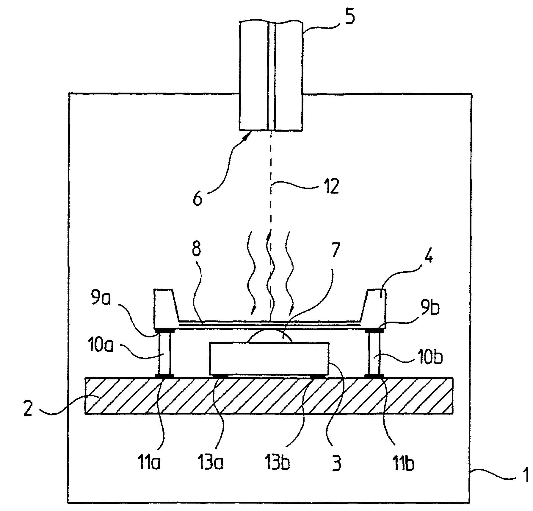
[0021]From the schematic illustration in FIG. 1, an optoelectronic transceiver according to the present invention will now be described.

[0022]A substrate element 2, embodied for instance as a printed circuit board, is disposed in a suitable housing 1. The elements of the present invention are disposed on the substrate element 2, and besides performing mechanical supporting and stabilizing functions, the substrate element 2 also serves to contact the optoelectronic components disposed on it. To that end, suitable conductor tracks, not visible in FIG. 1, however, are provided in the substrate element 2. As the essential components relative to the function of the optoelectronic transceiver according to the invention, a transmitting unit 3 and a receiving unit 4 are provided on the substrate element 2; they are oriented at a certain spatial relative orientation to an optical waveguide 5, or to its end face 6 that faces toward the optoelectronic transceiver. In this exemplary embodiment,...

second embodiment

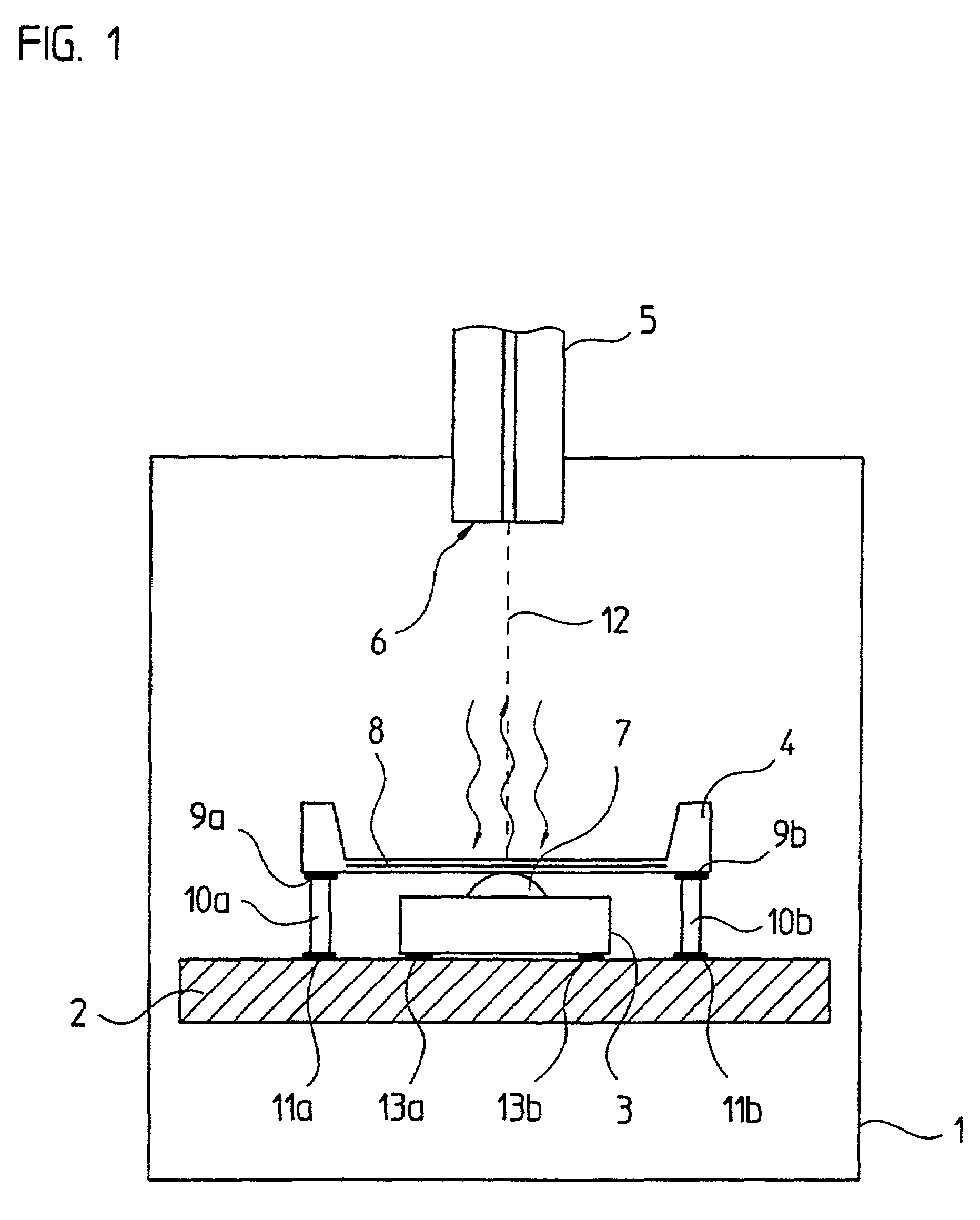
[0040]An alternative second embodiment of the apparatus of the invention is shown schematically in FIG. 2. It is essentially distinguished only in the manner of electrical contacting of the transmitting unit and receiving unit 103, 104 disposed on the substrate element 102 in the housing 101. While once again the contacting of the transmitting unit 103 is effected with the aid of the contacting elements 113a, 113b disposed on the back side, an alternative contacting variant is intended only for the receiving unit 104. Thus the receiving unit 104 is secured to the substrate element 102 via insulating elements 116a, 116b, while the contacting is done via bond wires 115a, 115b, which are disposed in the case of the receiving unit 104 on the side that faces counter to the radiation to be detected, or in other words its front side.

[0041]Otherwise, this embodiment of the apparatus of the invention again corresponds to the preceding variant in terms of the relative disposition of the vario...

third embodiment

[0042]the optoelectronic transceiver according to the invention is schematically shown in FIG. 3. Once again, this exemplary embodiment is distinguished from the preceding variants primarily in the selected manner of contacting the transmitting unit and receiving unit 203, 204, and merely offers certain advantages with regard to the possibly fully automatic SMD assembly.

[0043]Thus a substrate element 203 is now provided in the housing 201, and this element has an opening or recess 220 in a portion of it. Both the transmitting unit 203 and the receiving unit 204 are disposed in the region of this opening. The disposition of the transmitting unit 203 is done on the side of the substrate element 202 that is oriented facing away from the optical waveguide 205. The beam shaping optical element 207, embodied as a lens, is disposed in the region of opening 220.

[0044]The contacting of the transmitting unit 204 is done via contacting elements 2013a, 213b, which are disposed on the front side...


PUM


Abstract

An optoelectronic transceiver including an optoelectronic transmitting unit disposed along an optical axis and having a radiation-emitting layer region and an active radiation-sensitive layer region. The optoelectronic transceiver further including an optoelectronic receiving unit disposed along the optical axis and is disposed in bridge-like fashion above the optoelectronic transmitting unit. The optoelectronic receiving unit having an active radiation-sensitive layer region disposed perpendicular to the optical axis and located in a thin membrane, which is disposed immediately in front of the radiation-emitting layer region of the optoelectronic transmitting unit, and a radiation-emitting layer region.

Description

[0001]Applicants claim, under 35 U.S.C. § 119, the benefit of priority of the filing date of Jul. 29, 1998 of a German patent application, copy attached, Ser. No. 198 34 090.7, filed on the aforementioned date, the entire contents of which is incorporated herein by reference.BACKGROUND OF THE INVENTION[0002]1. Field of the Invention[0003]The present invention relates to an optoelectronic transceiver, or transmitting and receiving unit, as generically defined by the preamble to claim 1, which is suitable in particular for bidirectional data transmission by means of optical waveguides.[0004]2. Description of the Related Art[0005]For bidirectional data transmission via optical waveguides, optoelectronic transmitting units and receiving units or so-called transceivers are necessary on the various ends of the optical waveguides. One possibility for designing such transceivers is known for instance from European Patent Disclosure EP 0 410 143 A2. This reference provides that an optoelectr...

Claims


Application Information

Patent Timeline
IPC IPC(8): H04B10/00G02B6/42
CPCG02B6/4246H01L2224/48091H01L2924/10158H01L2224/73265H01L2924/00014
Inventor EISENBERGER, CHRISTIANPRONOLD, HERBERTSPECKBACHER, PETER
Owner DR JOHANNES HEIDENHAIN GMBH
Learn More