High performance flipchip package that incorporates heat removal with minimal thermal mismatch

a flipchip and heat removal technology, applied in the direction of semiconductor devices, electrical equipment, semiconductor/solid-state device details, etc., can solve the problems of lack of planarity and contact issues, difficult manufacturing, and relatively complex structure of some of these schemes, so as to reduce warpage during assembly, minimize interfacial stresses, and enhance the structure used

Inactive Publication Date: 2006-06-13
XILINX INC
View PDF36 Cites 76 Cited by
  • Summary
  • Abstract
  • Description
  • Claims
  • Application Information

AI Technical Summary

Benefits of technology

[0013]The present invention is directed to enhancing the structure used in making these packages to make the packages simpler to put together, reduce warpage during assembly, and minimize interfacial stresses without changing base function of the high performance package. The present invention provides an improved semiconductor package that minimizes the number of material types and interfaces required to implement heatsink in a thermally enhanced flipchip BGA package substrate. According to the invention, a single structure incorporating a cavity area for the die serves as both the support substrate and stiffener. The single rigid substrate with a cavity in which the die is mounted with flipchip interconnect addresses the stiffness function with a simple manufacturing step, and more importantly provides perfectly matched CTE between walls and floor of the package, so that it does not cause CTE interfacial reliability problems. Having matched CTE walls and floor of the cavity package allows the use of encapsulants without worrying about in-plane and z-axis CTE differences between the periphery of the cavity floor and the edge of the inner cavity wall.
[0014]The connecting points to the external balls end in an array of pads in the cavity area within the boundary of the die. This structural arrangement substantially eliminates interfacial stresses associated with adhesively attached stiffeners made from heterogeneous materials having different CTEs over the range of operating temperature. The single unitary structure includes cond...

Problems solved by technology

The thermo-mechanical impact of some of these schemes can be challenging due to the number of materials and interfaces involved.
A problem associated with most of these conventional high performance flipchip packaging structures is that the structure is relatively complex and can be difficult to manufacture.
The thermal interaction between these materials as the structures are exposed to the normal fabrication process temperatures can lead to warpage, lack of planarity and contact issues.
Furthermore, normal component mount reflow temperatures and subsequent temperature and power cycles experienced by ...

Method used


Image

  • High performance flipchip package that incorporates heat removal with minimal thermal mismatch
  • High performance flipchip package that incorporates heat removal with minimal thermal mismatch
  • High performance flipchip package that incorporates heat removal with minimal thermal mismatch

Examples


Embodiment Construction

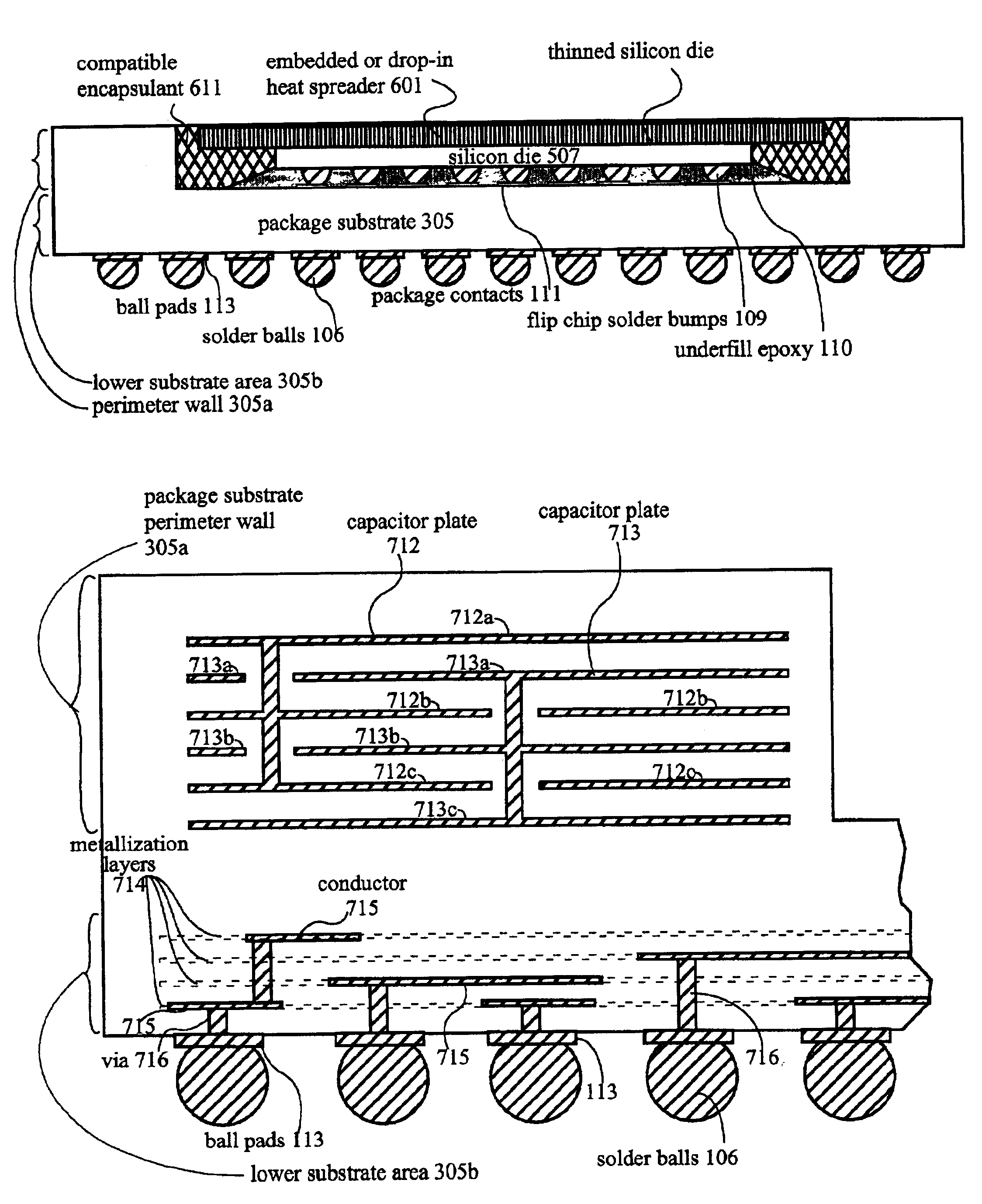
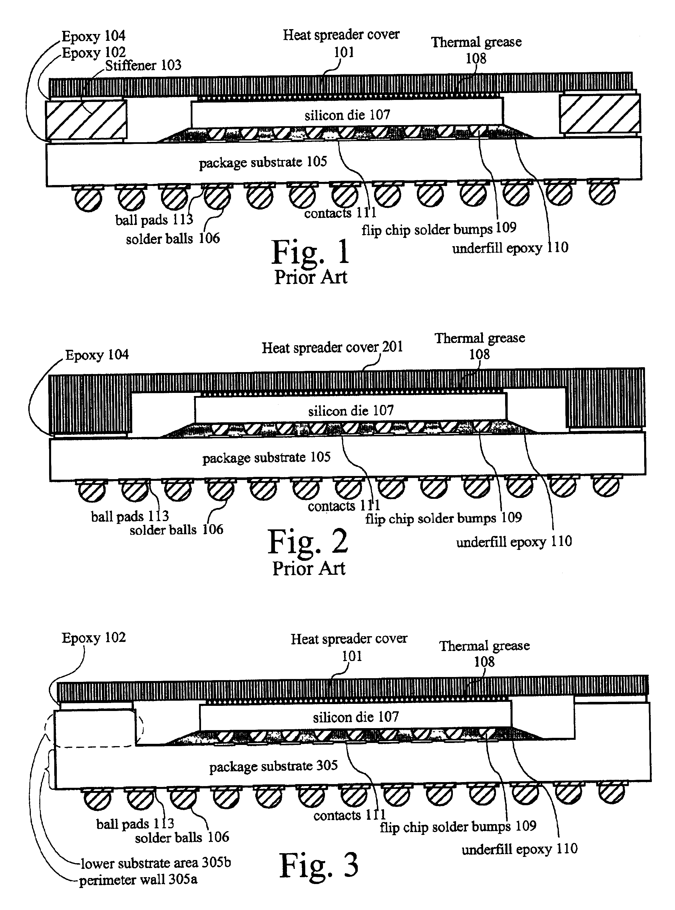
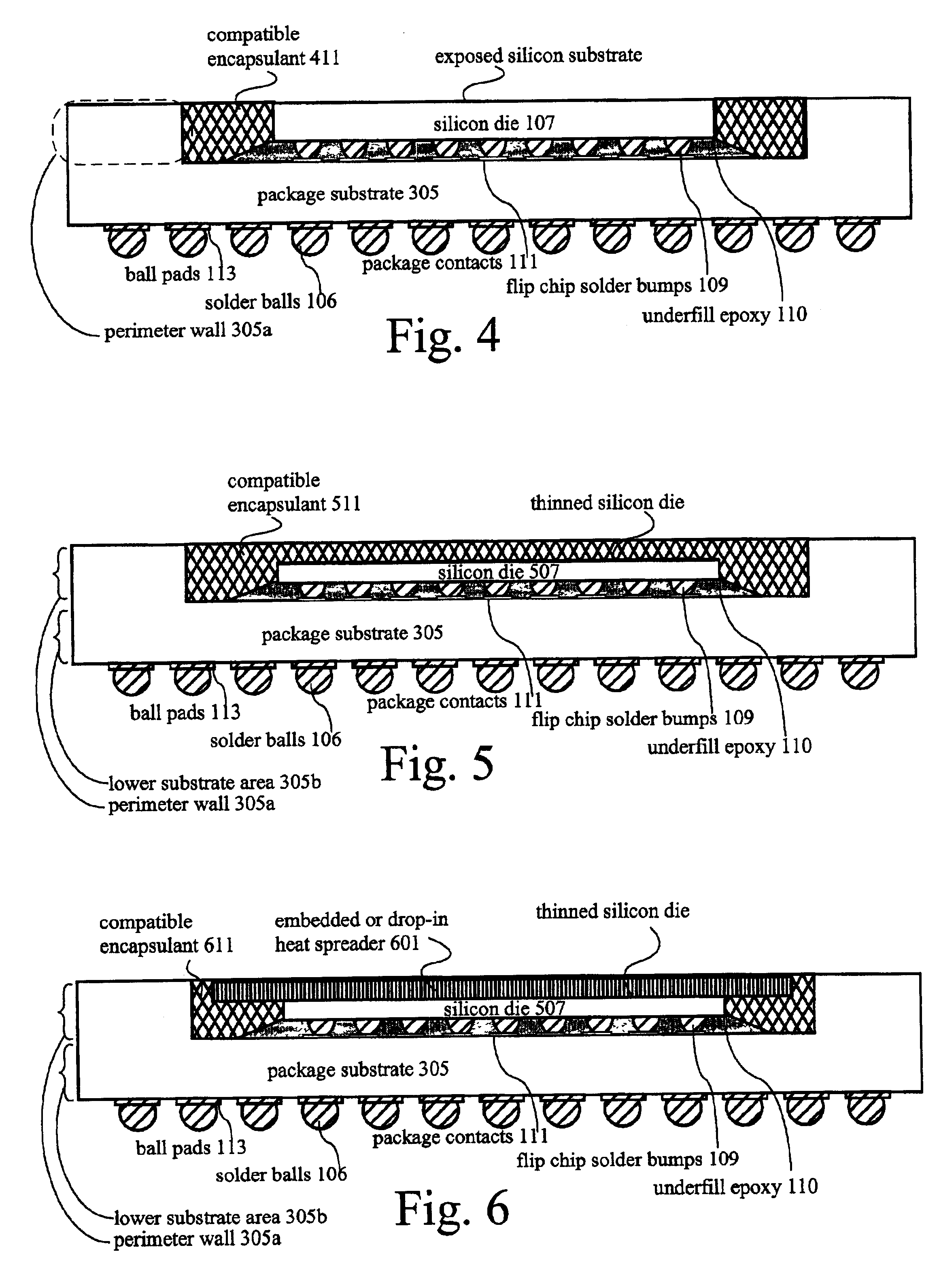
[0020]FIG. 3 shows one embodiment of the invention in which package 305 comprises a unitary structure having a central recessed region surrounded by perimeter walls 305a. Positioned within the central recessed region is silicon die 107 electrically connected to a plurality of contacts 111 in the central recessed region by solder bumps 109 and held in place by underfill epoxy 110. Unlike the prior art structures of FIGS. 1 and 2, package 305 is not just flat but incorporates the perimeter walls 305a as a single continuous piece with a lower substrate floor region 305b. The structure itself can have similar material characteristics to those used in prior art structures. A material laminate for package 305 may be procured from Kyocera, Japan as the HiTCE integrated circuit substrate with CTE of 12 ppm / ° C. In the package 305, as illustrated, the cavity floor interconnect metal is patterned to define an array of contact pads 111 that correspond to a similar arrangement of bumps 109 on t...


PUM


Abstract

A semiconductor flipchip package includes a central cavity area on the first major side for receiving a flipchip die therein. The package substrate is substantially made from a single material that serves as the support and stiffener and provides within the cavity floor all the connecting points for flipchip interconnection to the silicon die. The integral cavity wall serves as a stiffener member of the package and provides the required mechanical stability of the whole arrangement without the need for a separate stiffener material to be adhesively attached. The cavity walls may contain extra routing metallization to create bypass capacitors to enhance electrical performance. Optional methods to cover the silicon die enhance thermal performance of the package.

Description

FIELD OF THE INVENTION[0001]The invention relates to packaging of integrated circuits, particularly to flipchip-interconnected packaging that minimizes surface mount assembly temperature variations for a wide range of die sizes.BACKGROUND OF THE INVENTION[0002]Over the last few years, there has been a surge of activity geared to the use of flipchip interconnection in integrated circuits packages targeted for high performance applications such as networking, storage, and high end CPU computing. There are a number of reasons for this activity in flipchip-interconnected packages. One of the primary drivers spurring this high level of activity is the ability of flipchip interconnection to address pad limitation for these more I / O intensive integrated circuits. A modern integrated circuit die can integrate several million transistors together to form complex systems on a chip. Associated with these complex systems is the need to connect the signals and associated ground and multi-voltage...

Claims


Application Information

Patent Timeline
IPC IPC(8): H01L23/34H01L23/04H01L23/02H01L23/12H01L23/055H01L23/10H01L23/13H01L23/24H01L23/433H01L23/498
CPCH01L23/055H01L23/13H01L23/24H01L23/4334H01L23/49822H01L23/10H01L2924/18161H01L2224/16H01L2224/73204H01L2224/73253H01L2924/01057H01L2924/01079H01L2924/09701H01L2924/10253H01L2924/15153H01L2924/15165H01L2924/1517H01L2924/15311H01L2924/15787H01L2924/16152H01L2924/16195H01L2924/00014H01L2224/16227H01L2224/32225H01L2924/3511H01L2224/0401H01L2224/16225H01L2924/00
Inventor EGHAN, ABU K.HOANG, LAN H.
Owner XILINX INC
Why Eureka
Try Eureka