DC-DC converter
a dc converter and converter technology, applied in the direction of dc-dc conversion, dc amplifiers with modulator-demodulator, power conversion systems, etc., can solve the problems of difficulty in following the rapid change, low efficiency of the switching device, and drop in error amplifier output signal verr, so as to reduce the transient time of the output voltage and short period of time
- Summary
- Abstract
- Description
- Claims
- Application Information
AI Technical Summary
Benefits of technology
Problems solved by technology
Method used
Image
Examples
first embodiment
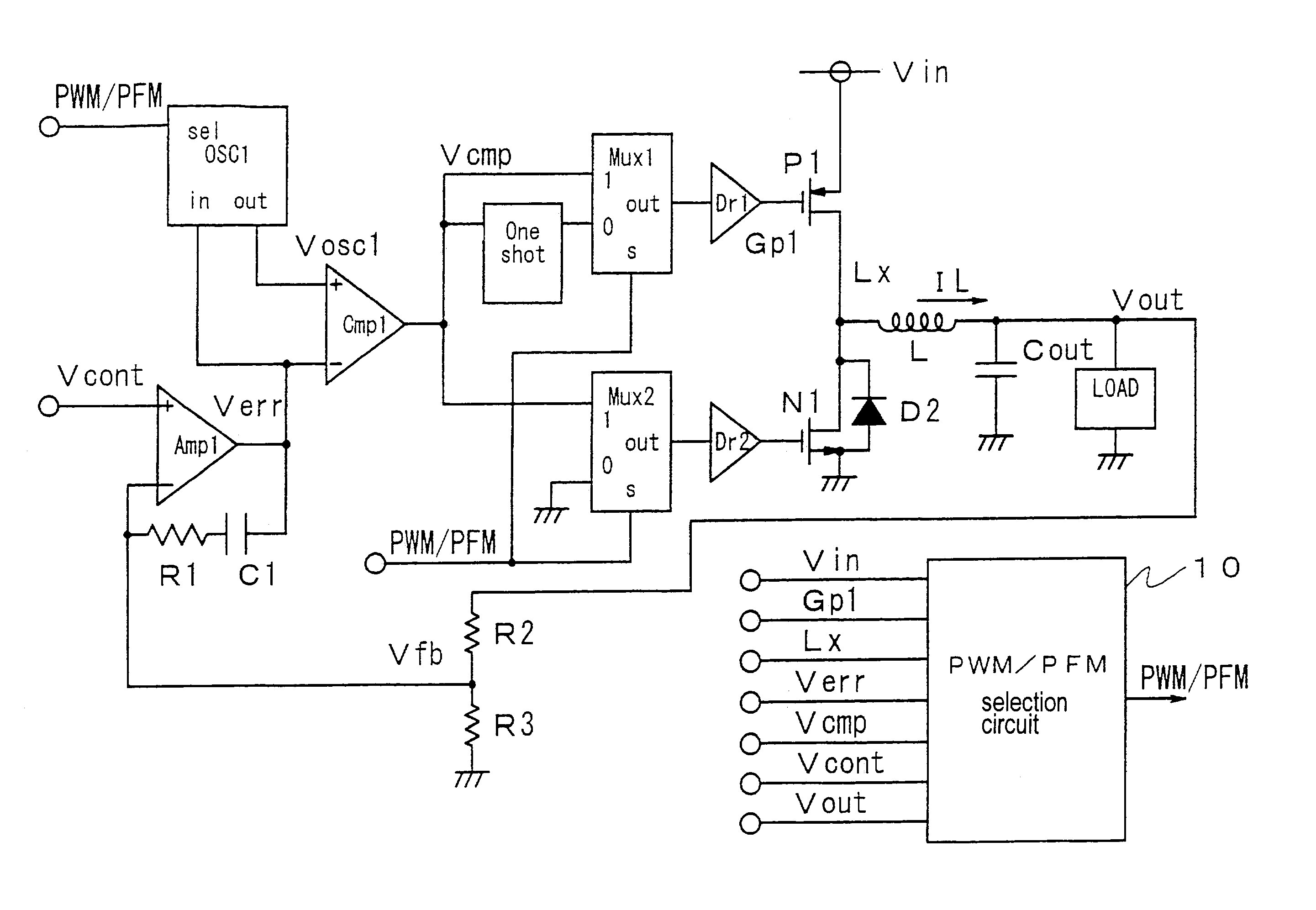
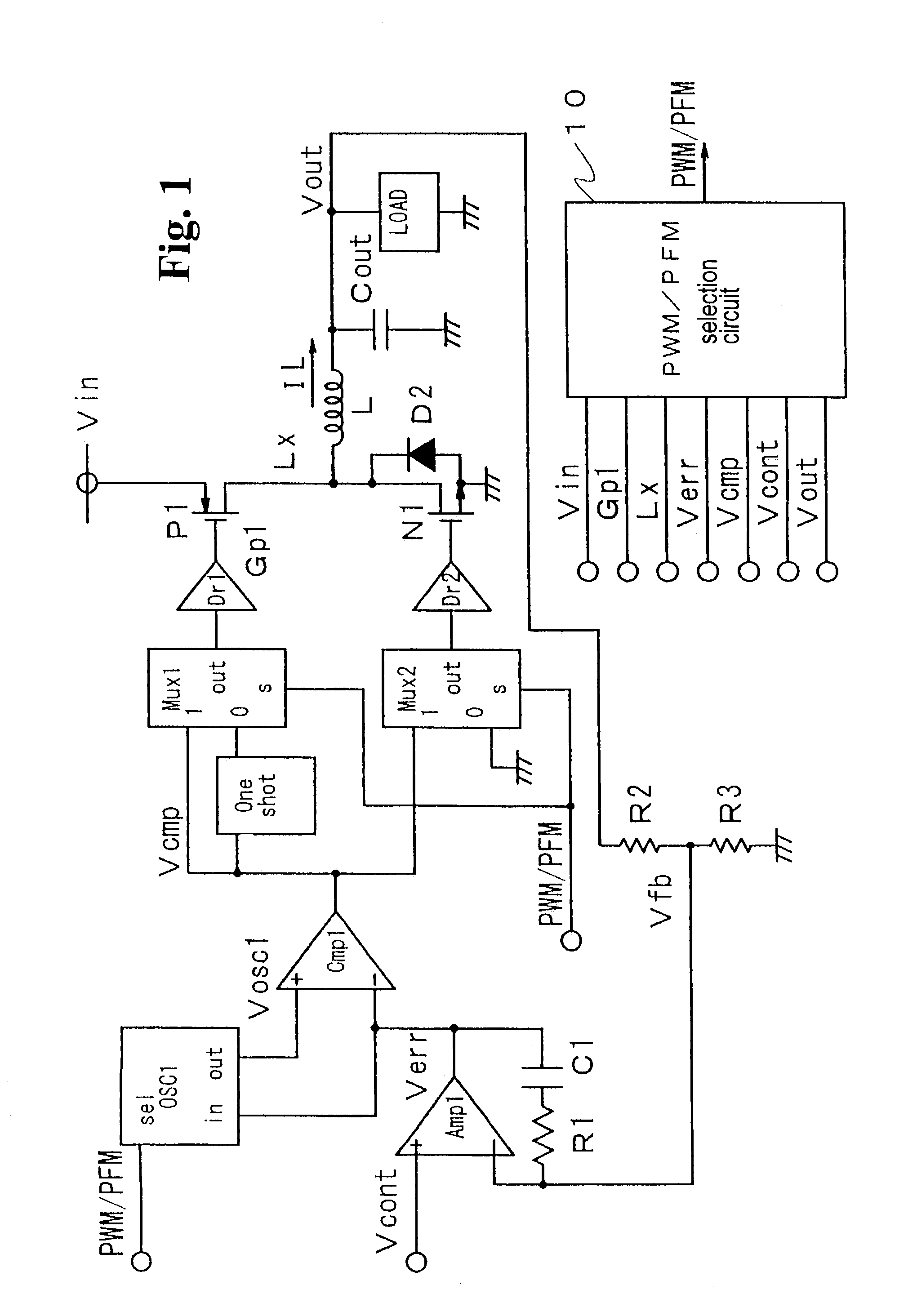
[0079]Hereunder, embodiments of the invention will be described in detail with reference to the accompanying drawings. FIG. 1 is a block circuit diagram of a DC—DC converter according to the invention. The DC—DC converter converts an input power supply voltage Vin to a certain voltage level and supplies the converted voltage to a load LAOD.
[0080]The DC—DC according includes an error amplifier (operational amplifier) Amp1, a capacitor C1 for phase compensation, a resistance R1 for phase compensation, a feedback resistance R2, a feedback resistance R3, an oscillator circuit OSC1, a comparator Cmp1 for pulse width modulation, a one-shot circuit one-shot, multi-plexer circuits Mux1 and Mux2, driver circuits Dr1 and Dr2, a p-channel transistor (MOSFET) P1 for outputting, an n-channel transistor (MOSFET) N1 for outputting, a choke coil L, a diode D2, a smoothing capacitor Cout, and a PWM / PFM selection circuit 10.
[0081]The PWM / PFM selection circuit 10 receives the input power supply voltag...
second embodiment
[0180]In the DC—DC converter according to the invention, the same effect can be expected when the PWM control mode is changed to the PFM control mode. It is assumed that the output voltage signal Vout is Vout3 in the PWM control mode, and the oscillation frequency changes to fosc2 in association with the changeover to the PFM control mode. When the control mode is changed from the PWM mode to the PFM mode at the time t2, the error amplifier output signal Verr, which is Vout3 initially, does not change sharply, and the p-channel transistor (MOSFET) P1 is switching at a frequency higher than the oscillation frequency fosc2. However, when the potential difference between Verr2 of the error amplifier output signal Verr and Verr3 thereof in the PWM control mode is small, it is possible to shorten the period for which the error amplifier output signal Verr reaches the potential Verr2 from the potential Verr3. Therefore, the overshooting in the PWM control mode is reduced.
[0181]As describe...
PUM
 Abstract
Description
Claims
Application Information


