
Array substrate having double-layered metal patterns and method of fabricating the same

a metal pattern and substrate technology, applied in the field of array substrates, can solve the problems of reducing the degree of image quality mixing damages and uneven etches the surface of the substrate, and affecting the stability of the liquid crystal display device, so as to increase the manufacturing yield and increase the manufacturing process stability

Active Publication Date: 2006-06-13
LG DISPLAY CO LTD
View PDF9 Cites 36 Cited by
  • Summary
  • Abstract
  • Description
  • Claims
  • Application Information

AI Technical Summary

Benefits of technology

The molybdenum alloy buffer layer ensures proper etching of the copper layer without damaging the substrate, enhancing the adhesion and stability of the metal patterns, thereby improving the manufacturing process and picture quality of liquid crystal display devices.

Problems solved by technology

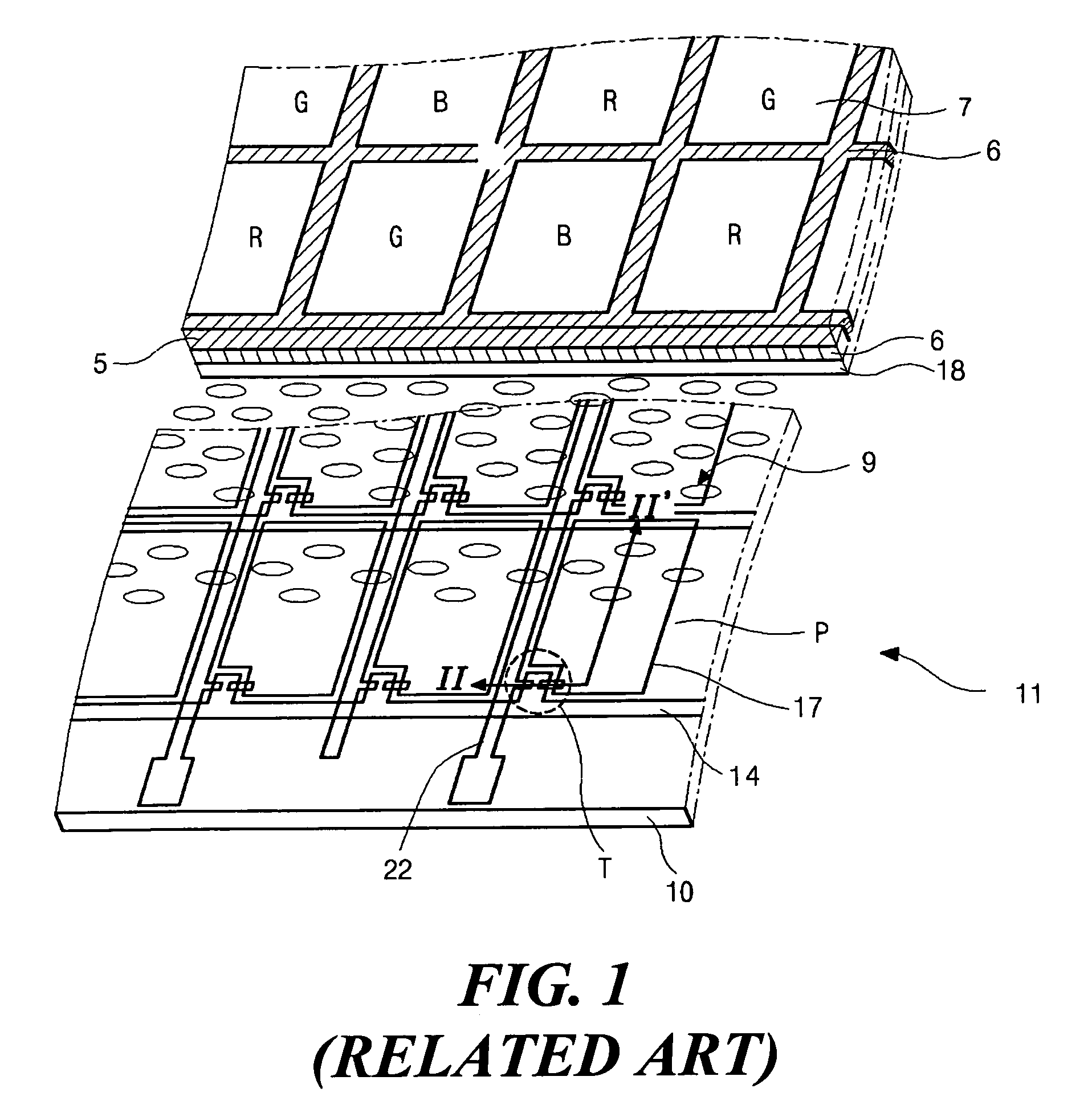
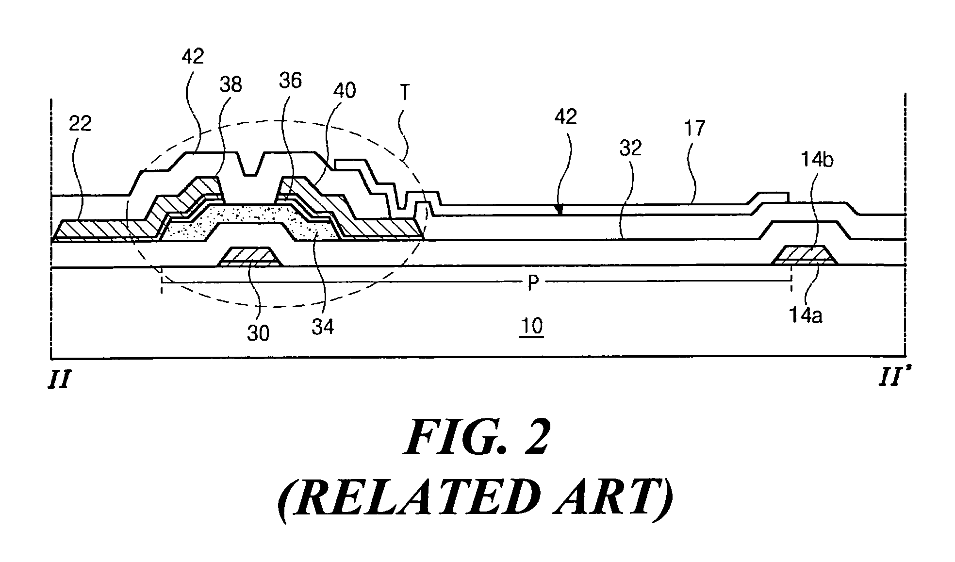
However, when etching the copper / titanium (Cu / Ti) double layers using the mixed solution of OXONE, hydrogen fluoride (HF) and ammonium fluoride (NH4F) to form the gate line and electrode, the mixture damages and unevenly etches the surface of the substrate due to that fact that F− ions are contained in the mixture solution.
As a result, the damages and uneven etch of the substrate surface cause a decreased degree of image quality in the liquid crystal display device, such as generation of stained and spotted images.
Furthermore, when the copper / titanium (Cu / Ti) double layers are applied for the data line, the source electrode and the drain electrode, the underlying gate insulation layer is definitely etched and damaged by the etchant.
Therefore, the damages and uneven etch of the gate insulation layer also cause the decreased degree of image quality in the liquid crystal display device.
These phenomena reduce the adhesion between the substrate and the copper / molybdenum (Cu / Mo) double-layered metal pattern and thus deteriorate stability of the liquid crystal display device.

Method used


Image

  • Array substrate having double-layered metal patterns and method of fabricating the same
  • Array substrate having double-layered metal patterns and method of fabricating the same
  • Array substrate having double-layered metal patterns and method of fabricating the same

Examples


Embodiment Construction

[0046]Reference will now be made in detail to the illustrated embodiments of the present invention, examples of which are illustrated in the accompanying drawings. Wherever possible, the same reference numbers will be used throughout the drawings to refer to the same or like parts.

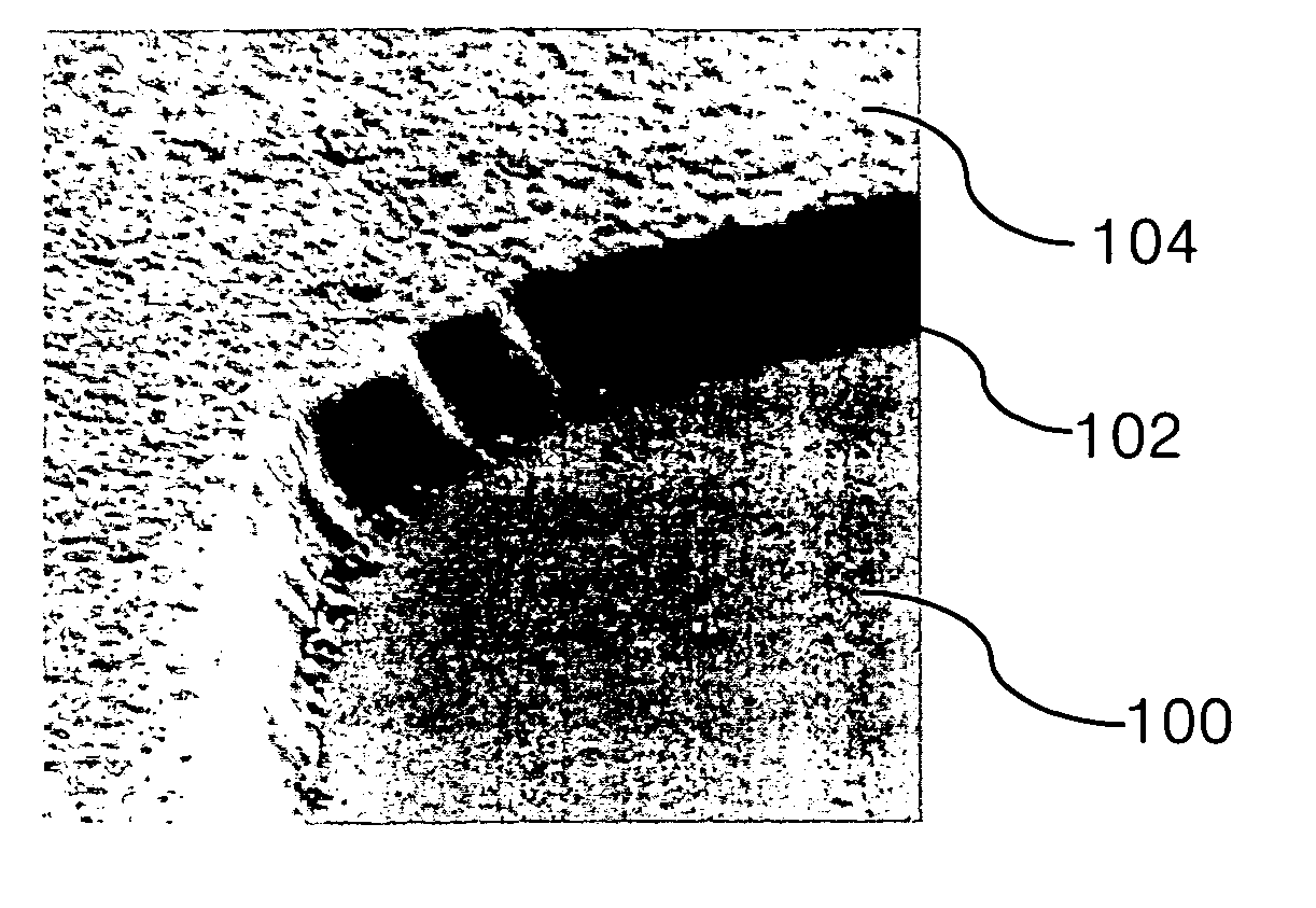
[0047]FIG. 7 is a photograph of partially-etched copper / molybdenum-alloy (Cu / Mo-alloy) double layers taken by a Scanning Electron Microscope (SEM). FIG. 8 is an enlarged view showing a portion of the etched copper / molybdenum-alloy (Cu / Mo-alloy) double layers of FIG. 7.

[0048]As shown in FIGS. 7 and 8, a molybdenum alloy (Mo-alloy) layer 102 is first formed on a substrate 100 and then a copper (Cu) layer 104 is sequentially formed on the molybdenum alloy (Mo-alloy) layer 102. Thereafter, the Mo-alloy layer 102 and the Cu layer 104 are patterned to form a Cu / Mo-alloy double-layered metal pattern. After patterning, a surface of the substrate 100 is smoothed, as indicated in FIG. 7. The Mo-alloy layer 102 is 10...


PUM

PropertyMeasurementUnit
thicknessaaaaaaaaaa
thicknessaaaaaaaaaa
thicknessaaaaaaaaaa

Abstract

An array substrate having double-layered metal patterns for use in a liquid crystal display device and a manufacturing method thereof are disclosed in the present invention. The array substrate includes a gate electrode and a gate line each having a molybdenum alloy (Mo-alloy) layer and a copper (Cu) layer configured sequentially on a substrate; a gate insulation layer on the substrate to cover the gate electrode and the gate line; an active layer arranged on the gate insulation layer in a portion over the gate electrode; an ohmic contact layer on the active layer; a data line on the gate insulation layer, the data line crossing the gate line and defining a pixel region; source and drain electrodes on the ohmic contact layer, the source electrode extending from the data line, and the drain electrode spaced apart from the source electrode; a passivation layer on the gate insulation layer covering the data line and the source and drain electrode, the passivation layer having a drain contact hole exposing a portion of the drain electrode; and a pixel electrode configured on the passivation layer in the pixel region, the pixel electrode electrically contacting the drain electrode through the drain contact hole.

Description

[0001]This application claims the benefit of the Korean Application No. P2002-0069285 filed on Nov. 8, 2002, which is hereby incorporated by reference for all purposes as if fully set forth herein.BACKGROUND OF THE INVENTION[0002]1. Field of the Invention[0003]The present invention relates to a liquid crystal display device, and more particularly, to an array substrate having double-layered metal patterns and a manufacturing method thereof. Although the present invention is suitable for a wide scope of applications, it is particularly suitable for increasing a picture quality in the liquid crystal display device and a process stability during the fabrication process.[0004]2. Discussion of the Related Art[0005]In general, since flat panel display devices are thin, light weight, and have low power consumption, they have been used for displays of portable devices. Among the various types of flat panel display devices, liquid crystal display (LCD) devices are widely used for laptop comp...

Claims


Application Information

Patent Timeline
Patent Type & Authority Patents(United States)
IPC IPC(8): G02F1/1343G02F1/136H01L21/20H01L29/04H01L31/20G02F1/1345G02F1/1362G02F1/1368H01L21/28H01L21/3205H01L21/77H01L21/84H01L23/52H01L27/12H01L29/423H01L29/49H01L29/786
CPCG02F1/136227G02F1/136286G02F1/1368H01L27/124H01L27/12G02F2001/136295G02F2001/13629G02F1/13629G02F1/136295G02F1/136
Inventor KWON, OH-NAMLEE, KYOUNG-MOOKCHOI, NACK-BONG
Owner LG DISPLAY CO LTD
Learn More