Projection exposure apparatus and method

a technology of projection exposure and projection, which is applied in the direction of photomechanical equipment, printing, instruments, etc., can solve the problems of uneven transfer of lines of a pattern designed to have an even line width, uneven amount of exposure light, and failure of the finished product, so as to improve the workability of the apparatus and improve the accuracy of exposur

Inactive Publication Date: 2006-06-13
NIKON CORP
View PDF26 Cites 57 Cited by
  • Summary
  • Abstract
  • Description
  • Claims
  • Application Information

AI Technical Summary

Benefits of technology

[0021]According to the projection exposure apparatus of the present invention, the contamination of the substrate-opposed surface of the optical member at the time of pattern transfer can be reduced and the exposure accuracy can be improved by, prior to the pattern transfer, removing the contaminants (e.g., a photosensitive agent), caused by the previous pattern transfer, on the substrate-opposed surface of the optical member arranged at the predetermined position in the vicinity of the exposure surface of the substrate.
[0059]According to the just described projection exposure method, prior to pattern transfer, the contamination inspection step is performed to inspect the optical member for contamination. In the judging step, based on the result obtained in the contamination inspection step, it is determined whether or not the contamination level of the optical member caused by the pattern transfer operations exceeds a predetermined permissible limit. When it is estimated that the contamination level of the optical member exceeds the predetermined permissible limit, the cleaning or replacement of the optical member is performed. When it is estimated that the contamination level of the optical member does not exceed the predetermined permissible limit, the pattern transfer is performed. In this manner, based on the result obtained in the contamination inspection step, it can be ensured that the optical member is cleaned or replaced with a new one at any time when it is required. Therefore, the exposure accuracy can be improved and the workability of the apparatus can also be improved.

Problems solved by technology

That is, regional unevenness in amount of exposure light may occur in the pattern transferred onto the substrate surface applied with a photosensitive agent.
As a result, for example, the line of a pattern designed to have an even line width may be transferred unevenly.
For the manufacture of an integrated circuit pattern, such uneven pattern line transfer may ultimately cause functional failure of the finished product.
Thus, the contamination of the optical member in the projection optical system is a serous problem.
Moreover, the use of an exposure illumination light with a shorter wavelength and a higher illuminance for the purpose of improving resolution and workability of the apparatus makes this problem more serious.
Therefore, there is a limitation in bringing the projection optical system close to the wafer at the time of pattern transfer.
In addition, because of the increased demand for high transfer accuracy, the installation repeatability for a replaceable contamination protection member and the permissible optical variability of the contamination protection member become very critical.
Therefore, the application of a cover glass (which has an even thickness) as the replaceable contamination protection means has its limit.
That is, when a contamination protection member is replaced with a new one, it is inevitable to re-adjust the total aberration balance of the projection optical system; which is not suitable for practical use.
Particularly, the transmittance of an S-polarized light (which is largely responsible for an imaging characteristic) is remarkably increased, resulting in poor imaging performance.
Moreover, a polymer film is generally difficult to be applied with an anti-reflection coating; which is not also suitable for practical use.

Method used


Image

  • Projection exposure apparatus and method
  • Projection exposure apparatus and method
  • Projection exposure apparatus and method

Examples


embodiment 1

[Embodiment 1]

[0088]The projection exposure apparatus and method according to the first embodiment of the present invention (Embodiment 1) will be illustrated below with reference to FIGS. 1–5.

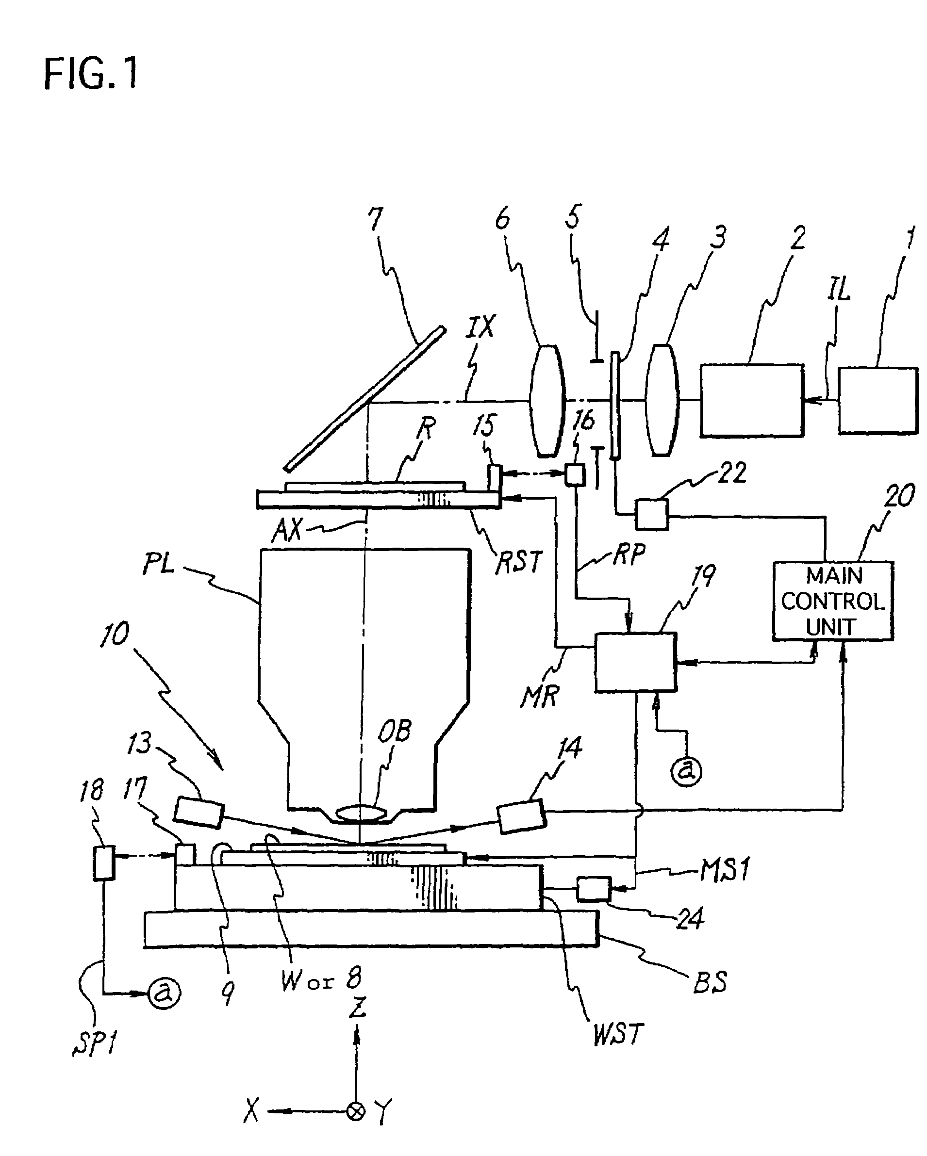
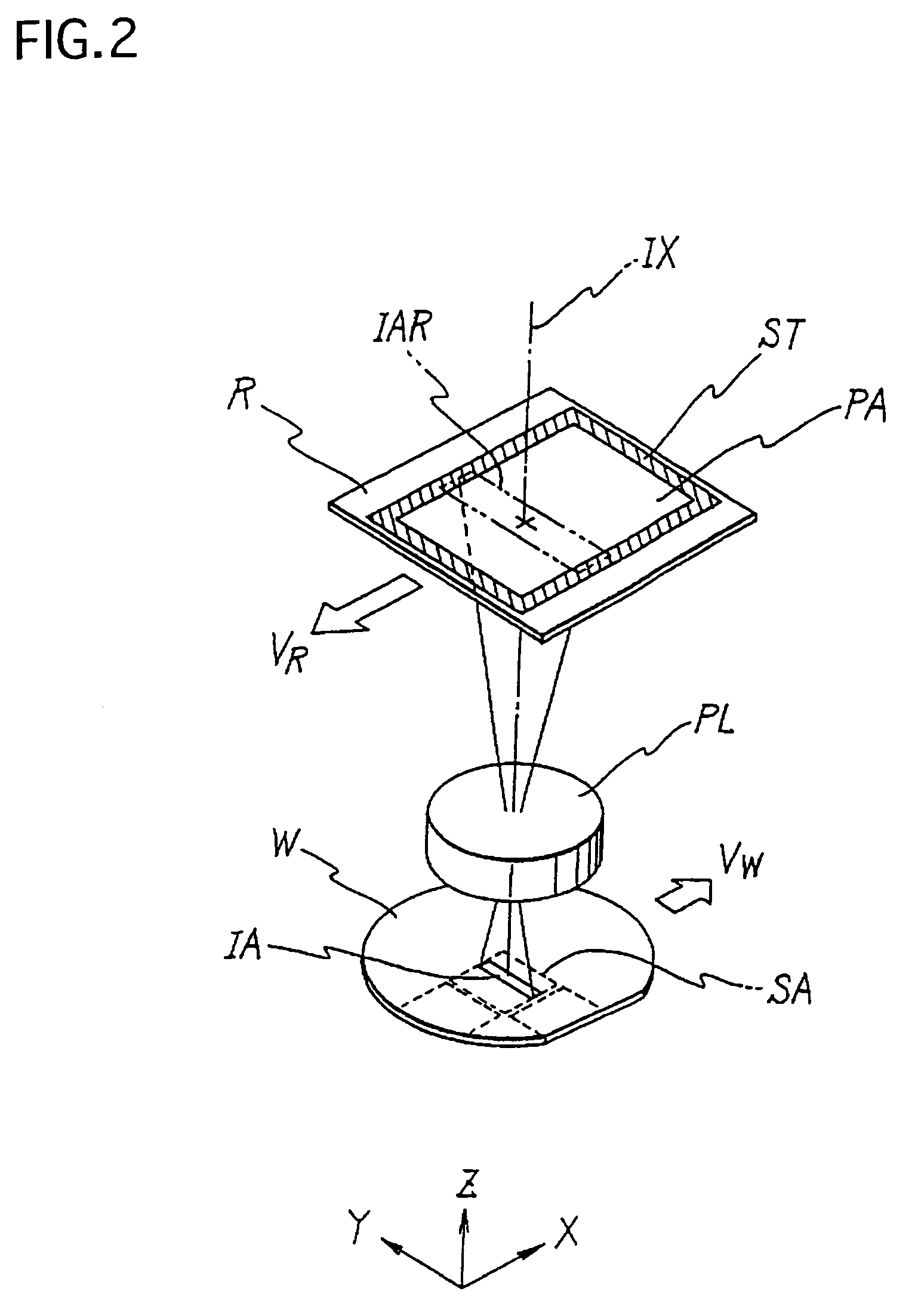
[0089]In the projection exposure apparatus of the present embodiment, pattern transfer onto a wafer W is performed, while cleaning an optical member (which is adapted to be disposed in the vicinity of the wafer W during pattern transfer) at the time when pattern transfer is not performed. A schematic illustration of the apparatus is presented in FIG. 1. The apparatus employs the so-called “step-and-scan” type of exposure mode.

[0090]As shown in FIG. 1, the apparatus comprises an illumination system comprising a light source 1 and an illumination optical system (including 2, 3 and 5–7); a reticle stage RST (i.e., a mask stage) for holding a reticle R (i.e., a mask); a projection optical system PL; a stage unit 10 which has a wafer stage WST for holding either a wafer W (i.e., a substrate) or a c...

embodiment 2

[Embodiment 2]

[0133]Hereinbelow, the projection exposure apparatus and method according to the second embodiment of the present invention (Embodiment 2) will be illustrated with reference to FIGS. 6 and 7. In the following description, the components similar to those described in Embodiment 1 above are denoted by the same reference numerals, and the overlapping explanatory descriptions are omitted.

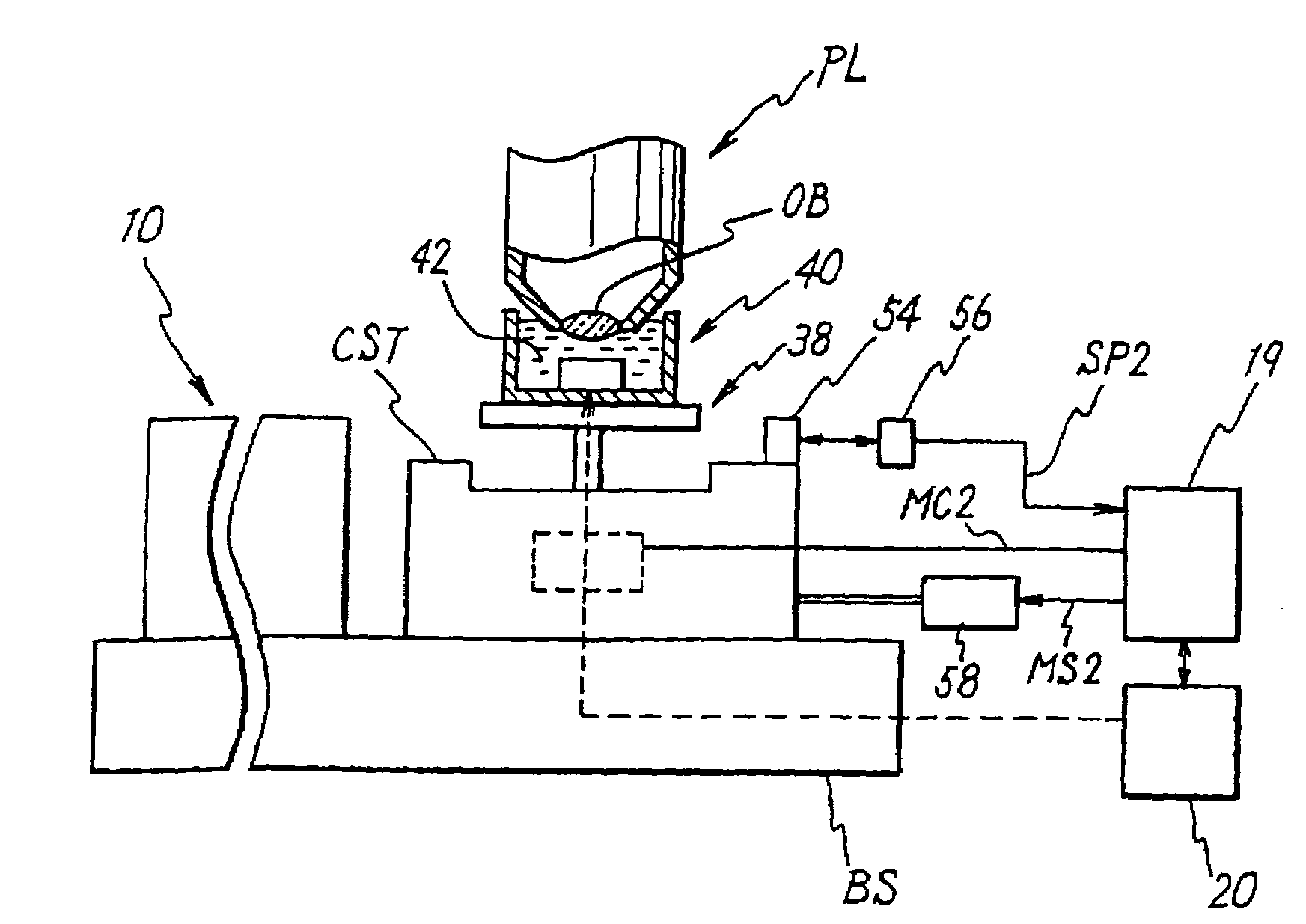
[0134]The projection exposure apparatus of the present embodiment is characterized in that, as a cleaning device, in place of the cleaning member 8 disposed on the wafer stage WST in the projection exposure apparatus of Embodiment 1, an ultrasonic cleaning device 40 (schematically shown in FIG. 6) is disposed on a cleaning stage CST distinct from the wafer stage WST. The objective lens OB of the projection optical system PL is cleaned by the ultrasonic cleaning device 40 at the time when pattern transfer is not preformed.

[0135]As shown in FIG. 6, the ultrasonic cleaning device 40 is provid...

embodiment 3

[Embodiment 3]

[0150]Hereinbelow, the projection exposure apparatus and method according to the third embodiment of the present invention (Embodiment 3) will be illustrated with reference to FIGS. 8 and 9. In the following description, the components similar to those described in the above embodiments are denoted by the same reference numerals, and the overlapping explanatory descriptions are omitted.

[0151]The projection exposure apparatus of the present embodiment is characterized in that, the cleaning member 8 in the projection exposure apparatus of Embodiment 1 shown in FIG. 1 is disposed on the cleaning stage CST which is distinct from the wafer stage WST as shown in FIG. 8. The objective lens OB of the projection optical system PL is cleaned using the cleaning member 8 at the time when pattern transfer is not preformed. In other words, in the present embodiment, the ultrasonic cleaning device 40 in Embodiment 2 is replaced with the cleaning member 8 of Embodiment 1.

[0152]As in t...


PUM

PropertyMeasurementUnit
wavelengthaaaaaaaaaa

Abstract

Pattern transfer can be performed with improved exposure accuracy, by reducing the contamination caused by the attachment of a photosensitive agent or the like on an optical member of a projection optical member or the like. The pattern transfer onto a substrate W is performed after cleaning the objective member OB disposed at a given position by a cleaning device 8 at the time when pattern transfer is not performed, or while making flow a gas in a space between the substrate W and the optical member OB by a contamination protection device 98. Alternatively, the optical member OB disposed at a given position is inspected for contamination by a contamination inspection device 84 at the time when pattern transfer is not performed, and the pattern transfer or the cleaning or replacement of the optical member is performed based on the result.

Description

[0001]This application is a Continuation of application Ser. No. 10 / 212,278 filed Aug. 6, 2002, ABN which is a DIV of Ser. No. 09 / 577,020 filed May 22, 2000, now U.S. Pat. No. 6,496,257, which is a CON of PCT / JP98 / 05258 filed Nov. 20, 1998.[0002]The present invention is based on the Japanese Patent Application Nos. 9-338109 and 10-83724, which are incorporated herein by reference in their entirety.FIELD OF THE INVENTION[0003]The present invention relates to a projection exposure apparatus and a projection exposure method. More specifically, the present invention relates to a projection exposure apparatus and a projection exposure method both useful for projection exposure of a pattern defined on a mask onto a substrate in the manufacture of a semiconductor device, a liquid crystal display device or the like by a photolithography process.BACKGROUND OF THE INVENTION[0004]In a projection exposure apparatus used in a photolithography process for the manufacturing a semiconductor device,...

Claims


Application Information

Patent Timeline
Patent Type & Authority Patents(United States)
IPC IPC(8): G03B27/52G01N21/00G03B27/42G03F7/20
CPCG03F7/2002G03F7/70241G03F7/70925G03F7/70916G03F7/70866
Inventor TANIGUCHI, TETSUOMURAYAMA, MASAYUKI
Owner NIKON CORP
Why Eureka
Try Eureka