Fabrication system and fabrication method

a technology which is applied in the field of fabrication system and fabrication method, can solve the problems of extremely difficult to process these semiconductor wafers under good management, extremely large number of semiconductor wafers processed simultaneously, and very complicated processing, so as to improve the percent non-defective, increase the number of products finished per unit time, and improve the effect of percent non-defectiv

Inactive Publication Date: 2006-06-13
RENESAS ELECTRONICS CORP
View PDF39 Cites 32 Cited by
  • Summary
  • Abstract
  • Description
  • Claims
  • Application Information

AI Technical Summary

Benefits of technology

[0015]An object of the present invention is to provide a fabricating system capable of shortening the term of a sequence of processes applied to works, making efficient use of processing apparatuses for enhancing the productivity while improving the percent non-defective thereby enlarging the number of products finished per unit time, and eliminating a clean space with a high cleanliness conventionally required; and a fabricating method using the system, which are particularly suitable for a semiconductor fabricating system and a fabricating method using the system mainly performed by single wafer processing and transporting.

Problems solved by technology

In some cases, the same apparatus is used for different processes, and thereby the repeating of the processing becomes very complicated.
Moreover, the number of semiconductor wafers processed simultaneously are extremely large.
It is extremely difficult to process these semiconductor wafers under good management.
As a result, there occur problems in that the appointed date is made longer, and the working ratio of each processing apparatus is reduced thereby lowering the number of products finished per unit time.
However, since many operators get around in a clean space in which processing apparatuses are disposed, dust adhering on the clothes of the operators and floors are scattered, which makes it difficult to keep the high cleanliness of the clean space.
This causes a disadvantage that the dust adheres on semiconductor wafers thereby reducing the percent non-defective.
However, this system is disadvantageous in that when the computer fails, the control of the fabricating system is stopped because of the absence of any means replaced with the computer.
Accordingly, in renewal of a processing apparatus, the software incorporated in the computer must be exceedingly corrected, thus requiring a large amount of labor for the correction and expansion of the software.
However, even when either of the above-described managing systems is used to automate the fabricating system, the effect of shortening the term of works and the effect of increasing the number of products per unit time by enhancing the working ratio and the percent non-defective do not reach the sufficient level for achieving the suitable time / suitable amount production.
However, even in the single wafer processing apparatus, so long as semiconductor wafers are processed for each unit of lot, one processing takes a time required to process the number of semiconductor wafers constituting one lot, which makes longer the waiting time until the subsequent processing.
Therefore, even if the management of products and processes is enhanced using computers, there is a limitation to the shortage of the term of works in principle.
Moreover, the waiting time between specified two continued processes is greatly dependent on the lot, that is, on the semiconductor wafer, thus obstructing the improvement in percent non-defective.
The second reason for this is that, it is very difficult to optimize a plurality of complicated processes even by the control using computers in the lot processing environment, thus reducing the productivity.
However, in some cases, the fabricating system cannot actually achieve the processing ability thus calculated as a whole.
Namely, it is impossible to optimize the complicated processes, the balance in the processing amount in each processing apparatus is not kept, thus reducing the productivity.
The fine pattern of a circuit element requires a high cleanliness, and it becomes difficult to realize a clean space with a high cleanliness, because the buildings having the clean space becomes very complicated and expensive, and a large energy is required to keep the clean space.
One of the disadvantage of the prior art fabricating system by the batch transporting is to require a clean space with a high cleanliness.
HEI 4-199709 has a disadvantage in increasing the number of processing apparatuses.
It is impossible to realize such a construction by the system shown in Japanese Patent Laid-open No.
The disadvantage of this system lies in that a plurality of semiconductor wafers are crossed to each other in processing apparatuses and transporters.
Only by connecting single wafer processing apparatuses to each other by means of a single wafer transporter, it cannot be achieved to obtain a high efficiency in simultaneously processing a plurality of semiconductor wafers.
To avoid the above problem, the processed amount must be reduced on the basis of the ability of the processing apparatus, which causes a disadvantage that the term of works is shortened and the wafer output is reduced.
In the single wafer transporting, the transporting is performed for each unit of a single wafer, so that it becomes very complicated.
The control and management for single wafer processing and single wager transporting are also complicated, and is very difficult to be satisfactorily realized.
The above-described prior art systems fail to examine this point, which is one reason why these systems are not extensively used.
The prior art managing system has the following problems.
The reason why such an auxiliary means is required is as follows: namely, the information to be managed in the system is large; and further, in the case that the management of information is all dependent on a computer for managing the information of the whole system, when there occurs the malfunction and system-down of the information managing computer, all of the management information in the fabricating system is lost, resulting in a large damage.
Moreover, since the renewing number of processing information necessary for processing in each processing apparatus becomes extremely larger than in the batch transporting, which causes a problem in that the management of information by the auxiliary storing means such as the IC card is large in the renewal frequency and is cannot be used.
In either method, the technique is limited only to the writing or reading of information, and it does not examine the management of information contained in a fabricating system.

Method used


Image

  • Fabrication system and fabrication method
  • Fabrication system and fabrication method
  • Fabrication system and fabrication method

Examples


embodiment 1

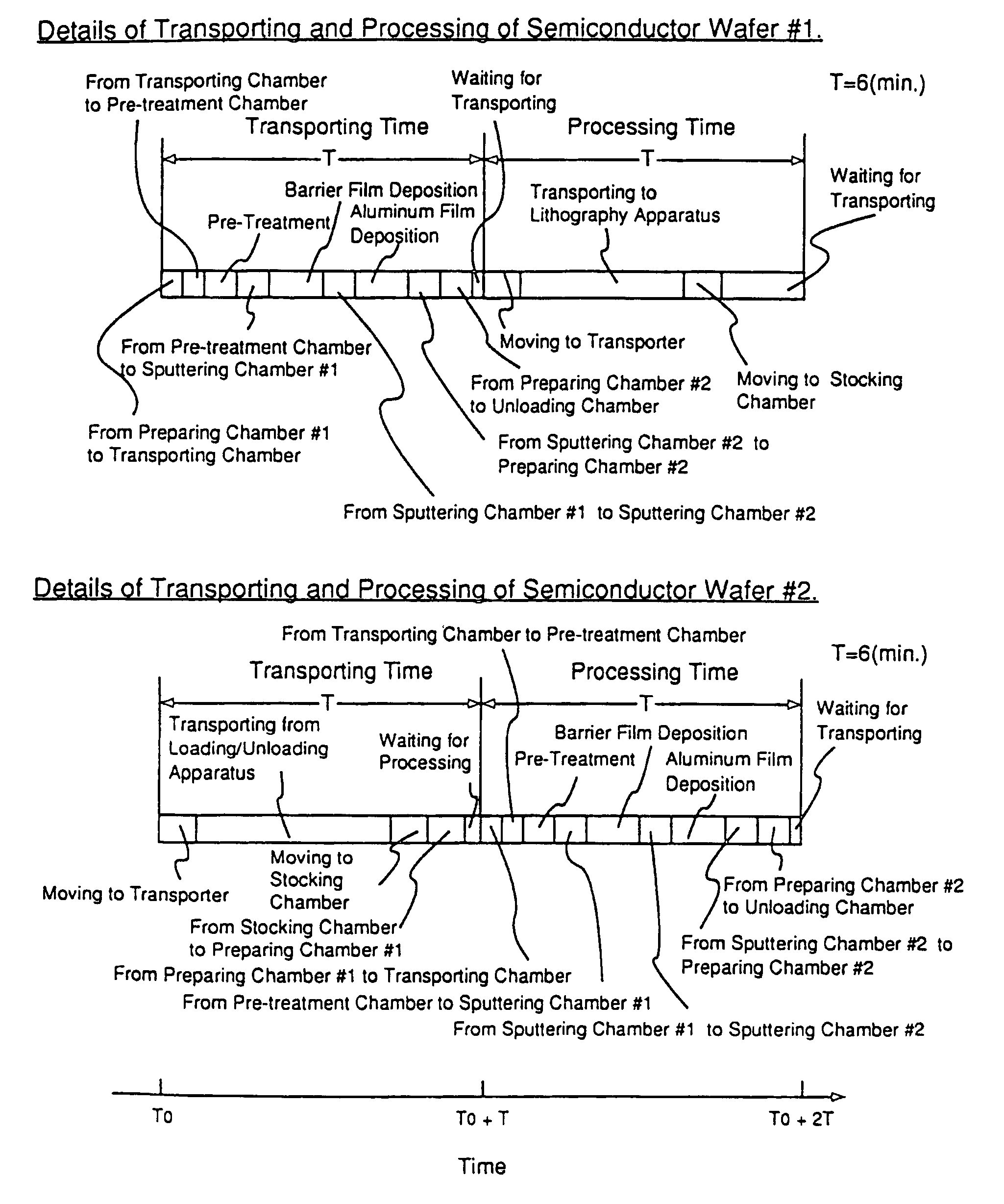
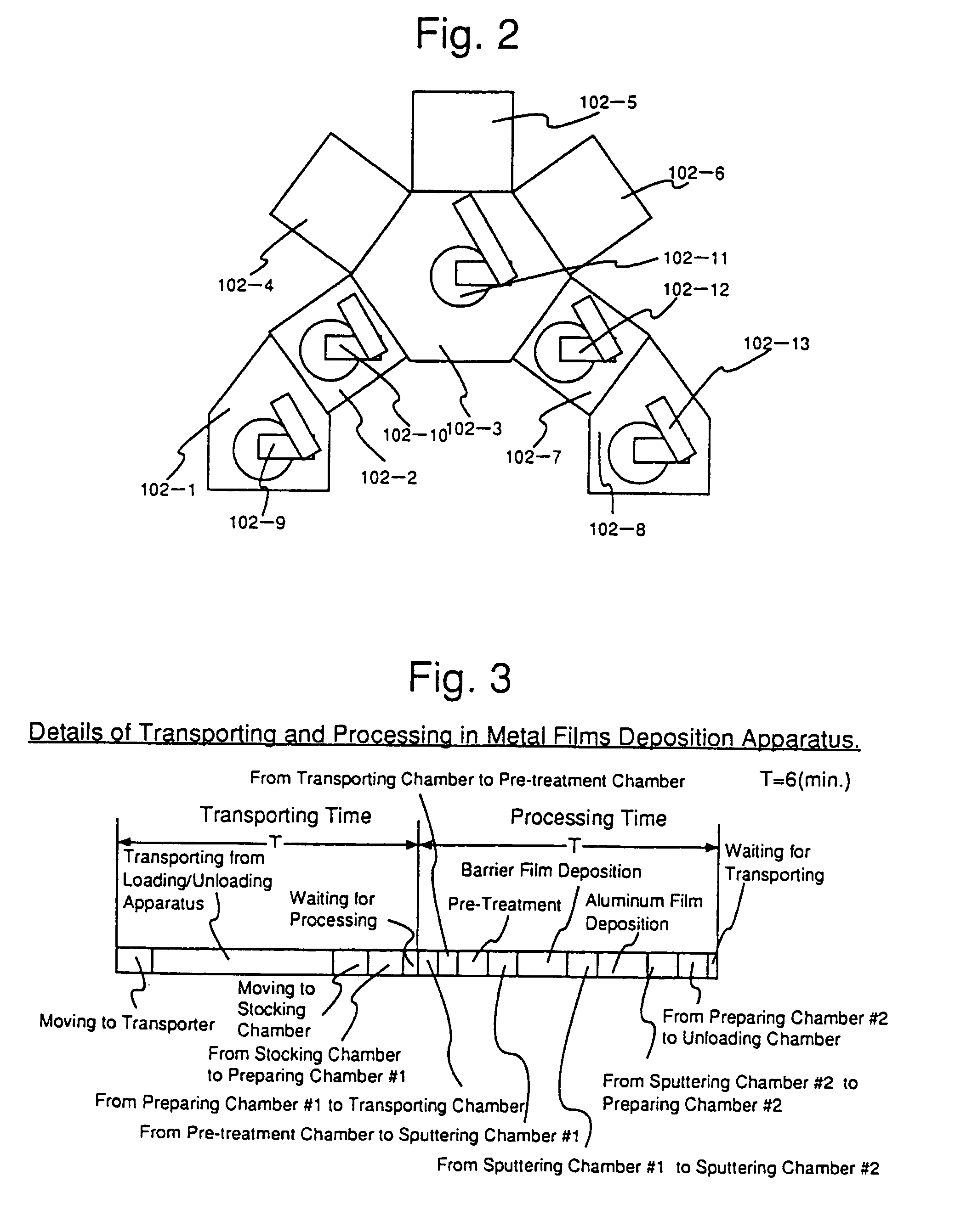
[0096]This will be described with reference to FIGS. 1 to 12 and Tables 1 and 3. In this embodiment, one layer metal film and a passivation layer are formed on a semiconductor wafer formed with elements and contact-holes.

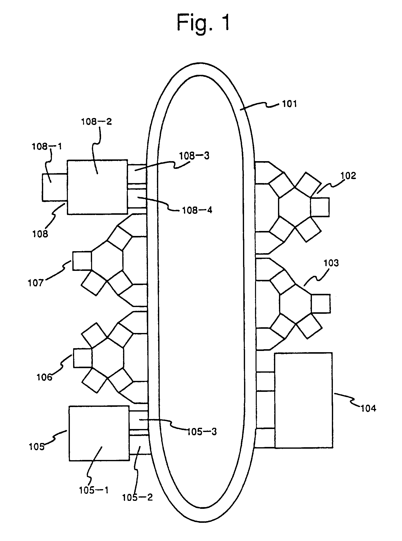
[0097]FIG. 1 is a view showing the embodiment of the inventive system. A metal film deposition apparatus 102, insulator film deposition apparatus 103, lithography apparatus 104, stocking apparatus 105, metal film dry etching apparatus 106, insulator film dry etching apparatus 107, and wafer loading / unloading mechanism 108 are disposed around a looped inter-apparatus single wafer transporter 101. Six pieces of semiconductor wafers #1 to #6 are continuously processed in the metal film deposition apparatus 102, lithography apparatus 104, metal film dry etching apparatus 106, insulator film deposition apparatus 103, lithography apparatus 104 and insulator film dry etching apparatus 107.

[0098]Six pieces of the semiconductor wafers are unloaded to the fabricating system b...

embodiment 2

[0125]This embodiment will be described with reference to FIGS. 1, 2, 7, 9, 11, 13 and 20. In this embodiment, the present invention is applied to a fabricating system and a fabricating method for fabricating an Si memory LSI, wherein a sequence of metallization processes for a CMOS-LSI having two layer metal films are applied to a wafer.

[0126]FIG. 13 is a view showing a fabricating system according to this embodiment. Lithography apparatuses 201 and 202 are adapted to perform a sequence of lithography processes including resist coating, resist baking, exposure using an infrared ray of mercury as a light source, resist developing and drying. By the provision of a plurality of processing apparatuses capable of applying the same processing, it becomes possible to effectively suppress the disorder of the processing due to a failure of the processing apparatus or the like.

[0127]The construction of each of the processing apparatuses 201 and 202 is the same as that of the lithography appa...

embodiment 3

[0143]This embodiment will be described with reference to FIGS. 21 and 22, and Table 5. In this embodiment, the present invention is applied to a fabricating system and a fabricating method for fabricating an Si memory LSI, wherein a sequence of processes for metallization of a CMOS LSI having a two layer metal film is applied to a wafer.

[0144]FIG. 21 is a view showing the fabricating system of this embodiment. Processing apparatuses 301 and 302 are adapted to perform a sequence of lithography processes including resist coating, resist baking, exposure using an i-ray of mercury as a light source, and resist developing. A processing apparatus 303 for dry-etching an interlayer insulator film is a cluster tool capable of dry-etching the SiO2 film or SiN4 film. It is provided with an ashing chamber 303-3 capable of removing the resist, other than two etching chambers 303-1 and 303-2. Each of the etching apparatuses 303-1 and 303-2 can perform the dry etching for the SiO2 film or SiN4 fi...


PUM

PropertyMeasurementUnit
timeaaaaaaaaaa
transporting speedaaaaaaaaaa
lengthaaaaaaaaaa

Abstract

Disclosed is a fabricating system including a plurality of processing apparatuses connected to each other by means of an inter-apparatus transporter, wherein one group of semiconductor wafers are processed in processing apparatuses and other group of wafers are transported to specified processing apparatuses for a time interval from (To+T) to a time To; and another group of wafers are processed and the remaining group of wafers are transported for a time interval from (To+T) to (To+2T). Since processing apparatuses can receive at least one of works from the inter-apparatus transporter for a time interval T min, the distribution of works from the transporter to processing apparatuses is completed for the time interval T min. The transporter is emptied for each time interval T min, and works are unloaded to the emptied transporter, which makes easy the scheduling, control and management of the transporting of a plurality of works in the fabricating system. Moreover, since the fabricating system including processing apparatuses is periodically controlled at a cycle time T min, the scheduling of a plurality of works can be made easy, to enhance the level of optimization, thus improving the productivity.

Description

[0001]This is a continuation application of U.S. Ser. No. 09 / 611,976, filed Jul. 6, 2000, now abandoned, which is a divisional application of U.S. Ser. No. 09 / 106,147 filed Jun. 29, 1998, now U.S. Pat. No. 6,099,598, which is a continuation application of U.S. Ser. No. 08 / 713,192, filed Sep. 12, 1996, now U.S. Pat. No. 5,820,679, which is a file wrapper continuation application of U.S. Ser. No. 08 / 274,308, filed Jul. 12, 1994, abandoned.BACKGROUND OF THE INVENTION[0002]The present invention relates to a fabrication system and a fabrication method capable of fabricating various kinds of semiconductor devices for a short period of time.[0003]In automated fabricating plants, various kinds of works are processed in a plurality of automated fabrication apparatuses. In such a fabricating plant, the scheduling of processing is determined in terms of the appointed data of works, working efficiency, and the minimized amount of semi-finished products between processing apparatuses. To smoothl...

Claims


Application Information

Patent Timeline
Patent Type & Authority Patents(United States)
IPC IPC(8): G06F19/00B65G49/07B23Q41/00B23Q41/02C23C14/56C23C16/54G05B19/418H01L21/00H01L21/02H01L21/027H01L21/205H01L21/285H01L21/304H01L21/3065H01L21/3205H01L21/677H01L21/68
CPCC23C14/568G05B19/41865H01L21/67161H01L21/67167H01L21/67173H01L21/67184H01L21/67276H01L21/67727H01L21/67745C23C16/54Y10T29/41G05B2219/45031Y10S414/137Y10S414/135Y10S438/908Y02P90/02H01L21/02
Inventor YOKOYAMA, NATSUKIKAWAMOTO, YOSHIFUMIMURAKAMI, EIICHIUCHIDA, FUMIHIKOMIZUISHI, KENICHIKAWAMURA, YOSHIO
Owner RENESAS ELECTRONICS CORP
Why Eureka
Try Eureka