Surface acoustic wave device, method of manufacturing the device, and electronic component using the device and method

Inactive Publication Date: 2006-06-20
PANASONIC CORP
View PDF20 Cites 4 Cited by
  • Summary
  • Abstract
  • Description
  • Claims
  • Application Information

AI Technical Summary

Benefits of technology

[0006]The present invention has for its object to provide, with a view to eliminating the drawbacks of prior art, a surface acoustic wave (SAW) device which efficiently uniformizes electric charge generated in a piezoelectric substrate by strain or heat treatment and uniformizes potential even after cutting of the substrate into a plurality of the SAW devices so as to prevent damage to electrodes and deterioration of electrical characteristics, its manufacturing method and an electronic component employing the SAW device.

Problems solved by technology

Thus, if electric charge becomes nonuniform among the electrodes, electric discharge occurs between the confronting interdigital transducers, between the confronting grating reflectors and between the interdigital transducer and the grating reflector, thereby resulting in damage to the electrodes or deterioration of characteristics of the SAW device.
However, in this conventional arrangement in which inside the dicing line, the short-circuiting thin line of the metallic thin film surrounds the interdigital transducer and the grating reflector and the thin lines electrically connect the short-circuiting thin line of the metallic thin film and the interdigital transducer, such disadvantages are incurred that since generated electric charge cannot be neutralized and uniformized sufficiently due to rise of impedance between lines in case the generated electric charge is large, in case a distance between the electrodes is short, in case the connected electrodes are far from each other, the line for connecting the short-circuiting thin line of the metallic thin film and the interdigital transducer is thin or in case the connecting line is a meander line or a portion of the connecting line is thinner than the remaining portion of the connecting line, damage to the electrodes and deterioration of electrical characteristics are caused by electrostatic discharge generated between the electrodes.

Method used


Image

  • Surface acoustic wave device, method of manufacturing the device, and electronic component using the device and method
  • Surface acoustic wave device, method of manufacturing the device, and electronic component using the device and method
  • Surface acoustic wave device, method of manufacturing the device, and electronic component using the device and method

Examples


first embodiment

(First Embodiment)

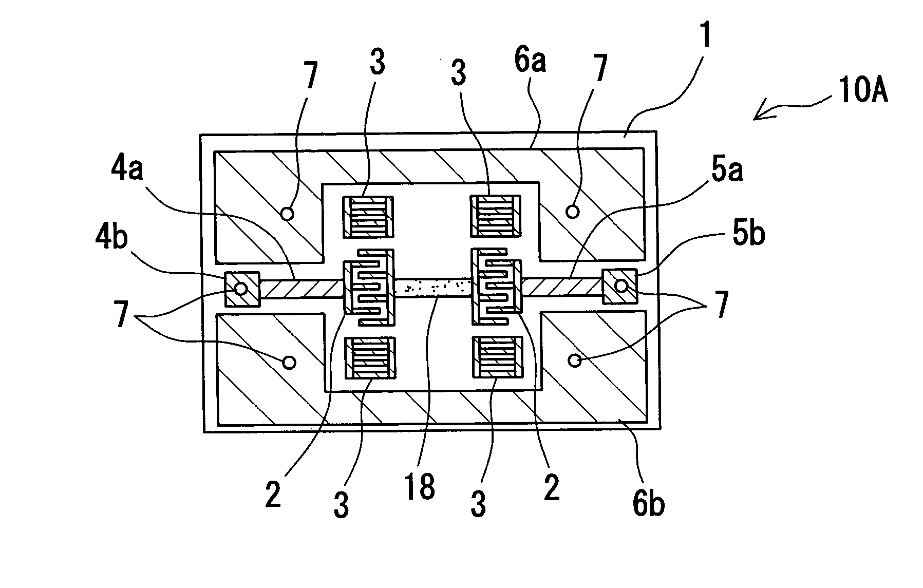
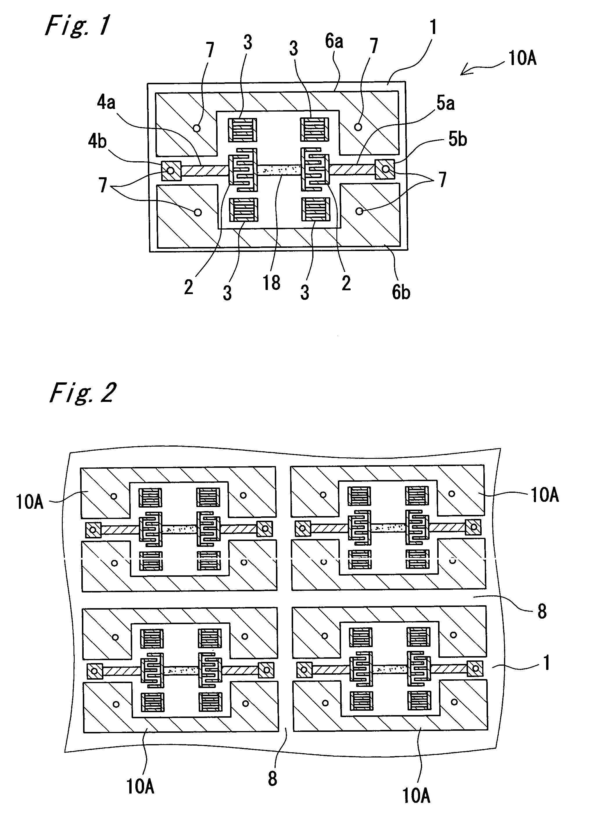
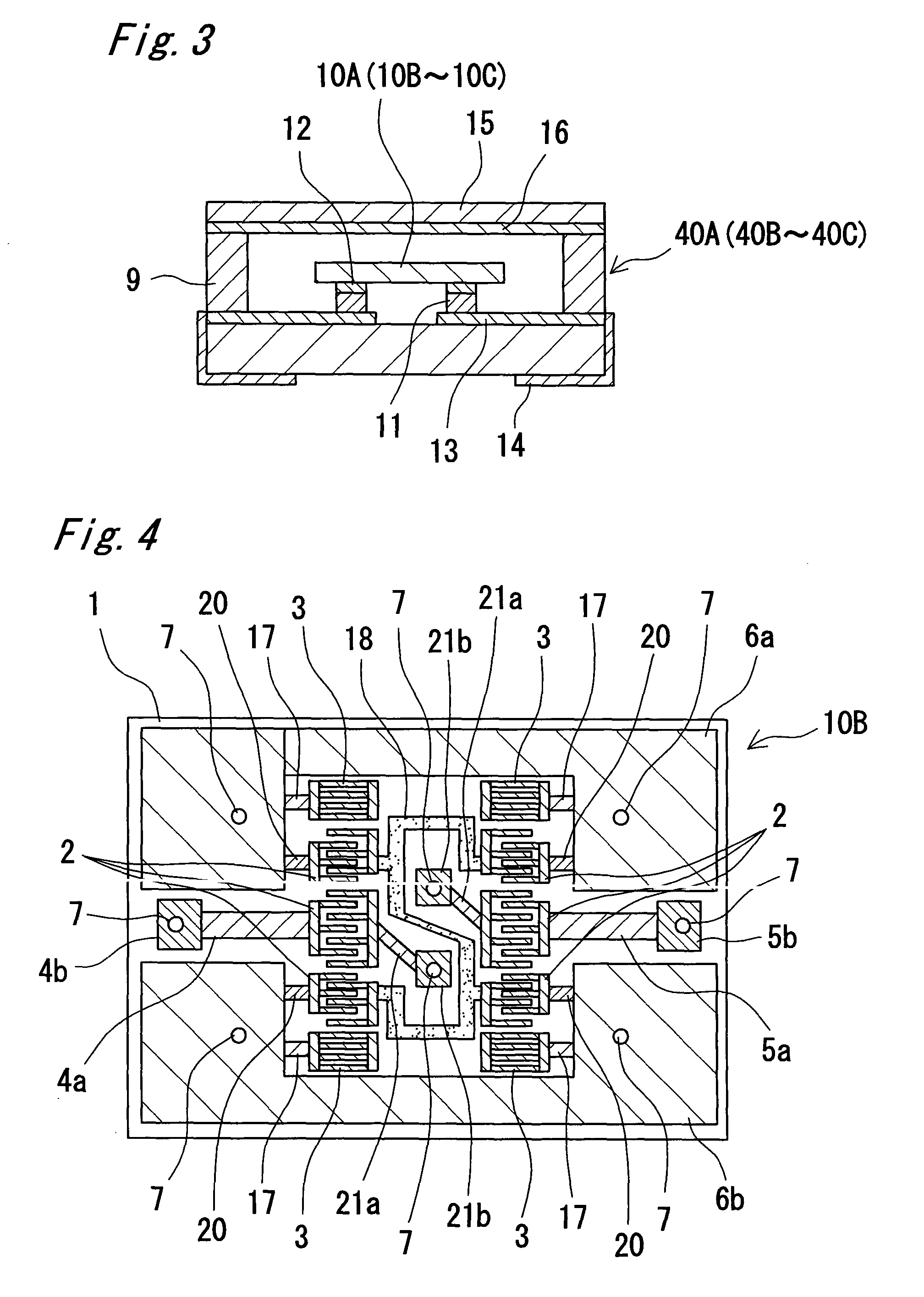
[0031]Hereinafter, Claims 1 to 5, 8 and 10 to 15 of the present invention are described by utilizing a first embodiment of the present invention. FIG. 1 is a top plan view showing an arrangement of an electrode pattern of a surface acoustic wave (SAW) device 10A according to the first embodiment of the present invention and FIG. 2 is a top plan view showing an arrangement of a plurality of the electrode patterns of FIG. 1 formed on a wafer. Meanwhile, FIG. 3 is a sectional view of an electronic component 40A in which the SAW device 10A is sealed in a package, etc. “1” is a piezoelectric substrate, “2” is a comb-shaped electrode, “3” is a reflector, “4a” is an input terminal lead-out electrode, “4b” is an input terminal electrode, “5a” is an output terminal lead-out electrode, “5b” is an output terminal electrode, “6a” and “6b” are auxiliary electrodes which are electrically independent of each other and have different widths locally, “7” is a bump, “8” is a region ...

second embodiment

(Second Embodiment)

[0065]Hereinafter, Claims 1 to 7 and 10 to 15 are described by utilizing a second embodiment of the present invention. FIG. 4 is a top plan view showing an arrangement of an electrode pattern of a SAW device 10B according to the second embodiment of the present invention. In FIG. 4, parts identical with those of FIG. 1 in the first embodiment are designated by identical reference numerals and the detailed description is abbreviated for the sake of brevity. Meanwhile, FIG. 4 shows an arrangement of the second embodiment schematically and does not illustrate relative ratio of respective dimensions.

[0066]FIG. 4 of the second embodiment is different from FIG. 1 of the first embodiment in that in FIG. 4, the reflector 3 is electrically connected to the auxiliary electrodes 6a and 6b by a plurality of beltlike electrodes 17 and the three comb-shaped electrodes 2 are provided for each of input and output terminals such that the two comb-shaped electrodes 2 disposed at op...

third embodiment

(Third Embodiment)

[0074]Hereinafter, Claims 1 to 5 and 9 to 15 of the present invention are described by utilizing a third embodiment of the present invention. FIG. 5 is a top plan view showing an arrangement of an electrode pattern of a SAW device 10C according to the third embodiment of the present invention. In FIG. 5, parts identical with those of FIG. 1 in the first embodiment are designated by identical reference numerals and the detailed description is abbreviated for the sake of brevity. FIG. 5 of the third embodiment is different from FIG. 1 of the first embodiment in that in FIG. 5, the reflector 3 is formed by a meander line and is electrically connected to the comb-shaped electrode 2. Meanwhile, FIG. 5 shows an arrangement of the third embodiment schematically and does not illustrate relative ratio of respective dimensions.

[0075]Namely, the comb-shaped electrode 2 and the reflector 3 are set in an electrically open state in the first embodiment, while the comb-shaped ele...


PUM


Abstract

A surface acoustic wave (SAW) device includes a comb-shaped electrode 2, a reflector 3 and a plurality of auxiliary electrodes 6a and 6b for surrounding the comb-shaped electrode 2 and the reflector 3, which are electrically independent of each other and have different widths locally. The SAW device is capable of efficiently and electrically uniformizing electric charge generated by pyroelectric property of a piezoelectric substrate 1.

Description

TECHNICAL FIELD[0001]The present invention relates to a surface acoustic wave (SAW) device, its manufacturing method and an electronic component employing the same.BACKGROUND ART[0002]In a conventional SAW device, after a metallic thin film has been formed on a whole surface of a piezoelectric substrate, a resist is coated on the metallic thin film and then, a desired electrode pattern is formed in which desired interdigital transducers and grating reflectors are not only surrounded by dicing lines but connected by thin lines through exposure, development and etching. The thus obtained article is cut along the dicing lines into a plurality of the SAW devices.[0003]In this method, once the SAW device has been cut from the piezoelectric substrate, the interdigital transducers and the grating reflectors are electrically separated from each other. Hence, upon application of heat or strain to the SAW device, electric charge is generated by pyroelectric property of the piezoelectric subst...

Claims


Application Information

Patent Timeline
IPC IPC(8): H03H9/25H03H3/08H03H9/02H03H9/64
CPCH03H3/08H03H9/02921H03H9/059H03H9/6473H03H9/25H03H9/6433H03H9/6463H03H9/1071H03H9/02913H01L2224/05568H01L2224/05573H01L2224/16225H01L2924/16195H01L2224/05624H01L2924/00014H01L2224/05647H01L2224/05655H01L2224/05666H01L2224/05671
Inventor IKEDA, KAZUONISHIMURA, KAZUNORIMURASE, YASUMICHI
Owner PANASONIC CORP
Why Eureka
Try Eureka