Method of fabricating high yield wafer level packages integrating MMIC and MEMS components

a technology of integrated circuits and components, applied in the field of integrated circuit fabrication techniques, can solve the problems of inability to reliably operate the mems device in the field, the difficulty of combining the two technologies, and the practical difficulties inherent in combining the two technologies, and achieve the effect of improving the circuit performan

Active Publication Date: 2006-06-27
NORTHROP GRUMMAN SYST CORP
View PDF20 Cites 47 Cited by
  • Summary
  • Abstract
  • Description
  • Claims
  • Application Information

AI Technical Summary

Benefits of technology

[0004]The present invention resides in a technique for integrating MMIC (monolithic microwave integrated circuit) technology with MEMS (micro electromechanical systems) technology in a double-wafer structure. Briefly, and in general terms, the method of the invention comprises the steps of providing a substrate wafer having a front face and a back face, and providing a cover wafer of comparable size to the substrate wafer; fabricating multiple MMIC and MEMS components on the front face of the substrate wafer; forming a first set of seal rings around selected device areas on the front face of the substrate wafer; forming a second set of seal rings on a surface of the cover wafer, in positions corresponding the first set of seal rings; and then bonding the first and second sets of seal rings to provide a double-wafer structure that includes multiple device cavities formed between the substrate wafer and the cover wafer. The ensuing steps include thinning the substrate wafer by removing material from its back face; and completing the MMIC and MEMS fabrication on the back face of the thinned substrate wafer. Integration of MMIC and MEMS components provides enhanced circuit performance for each fabricated device.
[0006]In accordance with one important aspect of the invention, the method further comprises forming a continuous guard ring surrounding the multiple device cavities in the double-wafer structure. More specifically the step of forming a continuous guard ring comprises forming one component of the guard ring on the cover wafer and another component on the front face of the substrate wafer, and then bonding the guard ring components together, simultaneously with the step of bonding the first and second sets of seal rings together. The continuous guard ring provides mechanical support to the substrate wafer during the thinning step, resulting in high production yields, and protects the MMIC and MEMS components during processing steps performed in completing the MMIC and MEMS fabrication.

Problems solved by technology

Moreover, MEMS devices cannot operate reliably in the field without hermetic packaging.
There are, however, practical difficulties inherent in combining the two technologies.
A related goal is to achieve cost savings of the type normally associated with wafer-level fabrication and packaging of integrated circuitry, but in this case rendered very difficult to achieve by the thin substrate structure of MMIC components.

Method used


Image

  • Method of fabricating high yield wafer level packages integrating MMIC and MEMS components
  • Method of fabricating high yield wafer level packages integrating MMIC and MEMS components
  • Method of fabricating high yield wafer level packages integrating MMIC and MEMS components

Examples


Embodiment Construction

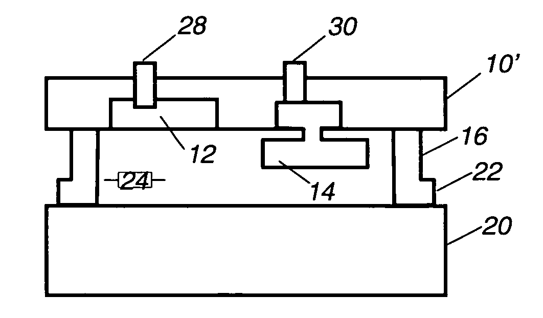
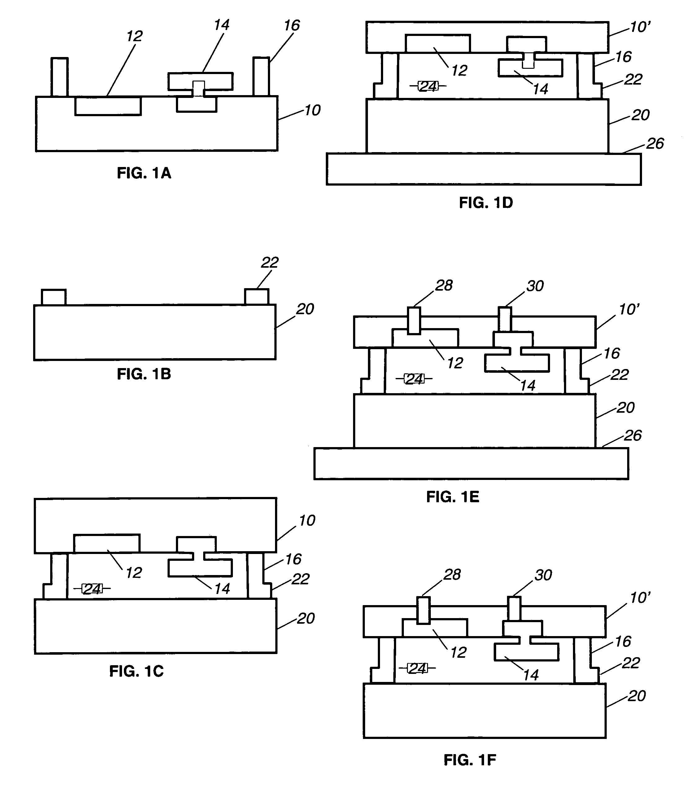
[0017]As shown in the drawings for purposes of illustration, the present invention concerns a process for wafer-level fabrication of circuitry that integrates MMIC (monolithic microwave integrated circuit) technology and MEMS (micro electromechanical systems) components. Although significant performance benefits can be achieved by this integration of technologies, differences in their fabrication and packing requirements have made this goal an elusive one for designers. One difficulty in particular is that production yields are rendered extremely low because of the required thinness of a MMIC substrate and a resultant tendency of the substrate to crack or break during wafer-level fabrications steps.

[0018]In accordance with the present invention, MMIC and MEMS components are integrated into a double-wafer structure that overcomes the foregoing difficulties. The principles of the fabrication process are shown in diagrammatic form in FIGS. 1A–1F. In particular, FIG. 1A shows the cross ...


PUM


Abstract

Monolithic microwave integrated circuit (MMIC) components and micro electromechanical systems (MEMS) components are integrated onto a single substrate at a wafer scale, by first performing MMIC and MEMS fabrication on a front face of a thick substrate wafer, bonding the substrate wafer to a cover wafer, thinning the back face of the substrate wafer and, finally, completing MMIC and MEMS fabrication on the back face of the thinned substrate wafer. The fabrication process is facilitated by use of a guard ring between the wafers to provide additional mechanical support to the substrate wafer and to protect the devices while the MMIC / MEMS fabrication is completed, and by a low temperature bonding process to join the substrate wafer and the cover wafer at multiple device cavity seal rings.

Description

[0001]This invention was made with Government support under contract number DAAD17-02-D-0002 awarded by the United States Army. The Government has certain rights in this invention.BACKGROUND OF THE INVENTION[0002]This invention relates generally to integrated circuit fabrication techniques and, more particularly, to methods for integrating monolithic microwave integrated circuit (MMIC) and micro electromechanical systems (MEMS) components into a single package. MMIC technology necessitates the use of an extremely thin substrate, in the range of 50–100 μm, and a MEMS device necessarily has significant thickness because it is basically a three-dimensional device. Moreover, MEMS devices cannot operate reliably in the field without hermetic packaging.[0003]Integration of MEMS devices, such as radio frequency (RF) MEMS switches, with MMIC technology offers significant system performance improvements, such as low loss, high linearity and added functionality, in many space and military app...

Claims


Application Information

Patent Timeline
Patent Type & Authority Patents(United States)
IPC IPC(8): H01L21/30B81C99/00
CPCB81B7/0064H01L25/16H01L23/66B81C2203/0118B81C2203/019H01L2924/0002H01L2223/6683H01L2924/00
Inventor CHANG-CHIEN, PATTY P.TOMQUIST, KELLY J.GEIGER, CRAIG B.KONG, ALVIN M.
Owner NORTHROP GRUMMAN SYST CORP
Why Eureka
Try Eureka