
Gap fill for high aspect ratio structures

a technology of high aspect ratio and filling, applied in the direction of coating, chemical vapor deposition coating, metallic material coating process, etc., can solve the problems of reducing budgets, void-free filling of high aspect ratio spaces (e.g., ar>3.0:1) becoming increasingly difficult, and the top part of a high aspect ratio structure sometimes closes, so as to reduce side-wall dielectric redeposition, increase flow rate, and effect of growing a dielectric film

Inactive Publication Date: 2006-06-27
NOVELLUS SYSTEMS
View PDF91 Cites 17 Cited by
  • Summary
  • Abstract
  • Description
  • Claims
  • Application Information

AI Technical Summary

Benefits of technology

[0010]One aspect of the invention provides a method of filling gaps on a semiconductor substrate. The method may be characterized by the following sequence: (a) providing a substrate in a process chamber of a high density plasma chemical vapor deposition reactor; (b) introducing a process gas including at least hydrogen into the process chamber; and (c) applying a bias to the substrate. This method will effectively grow a dielectric film on the semiconductor substrate via HDP CVD. This process effectively fills gaps having widths of less than about 1.5 micrometer.
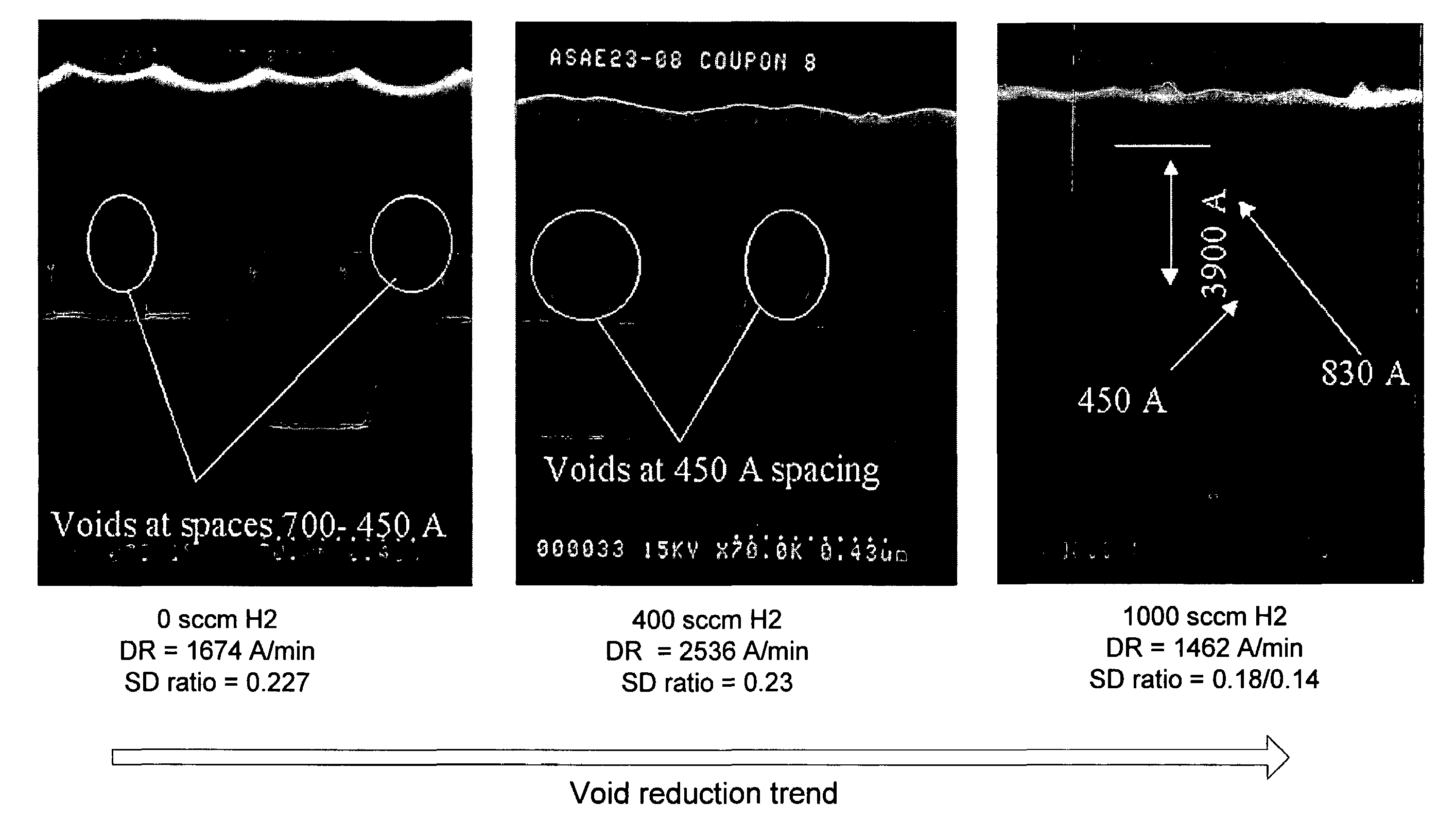
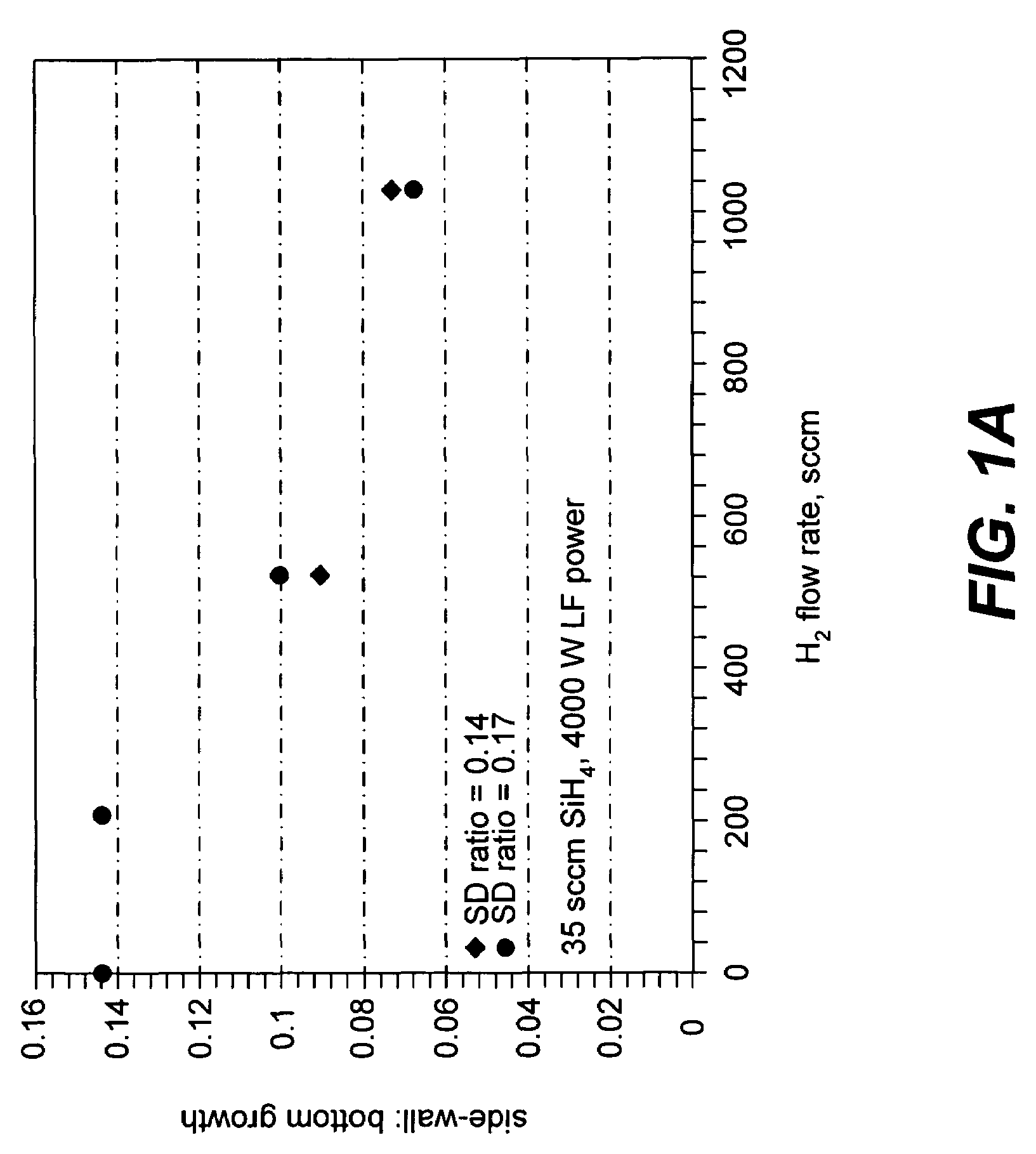
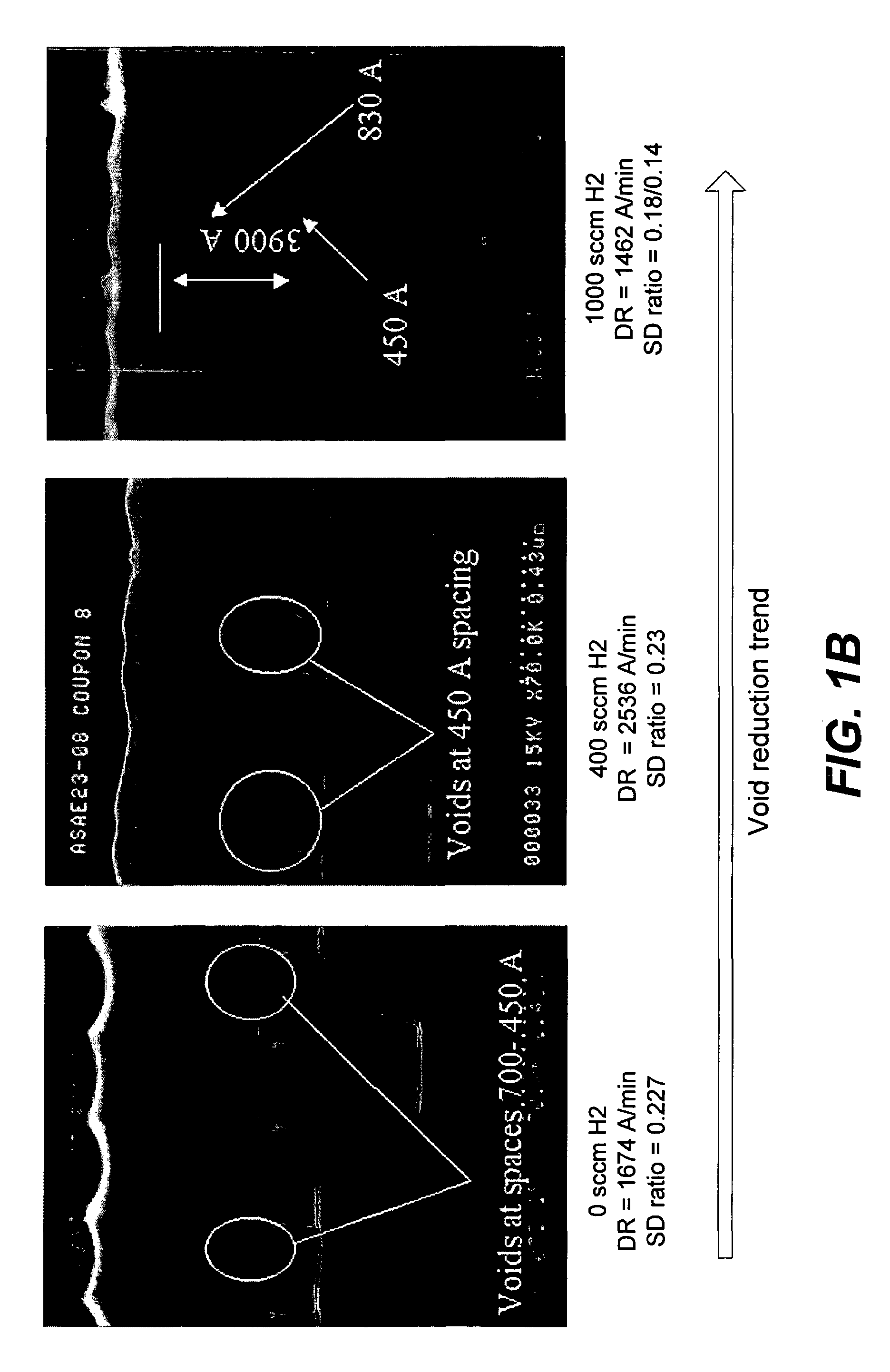
[0011]The process gas preferably provides hydrogen at a flow rate of at least about 400 sccm. This value is based on a 200 millimeter substrate. Larger substrates may require correspondingly higher flow rates. The inventors have found that hydrogen flow rates in this regime provide significantly reduced side-wall dielectric redeposition during HDP CVD.
[0012]In an alternative preferred embodiment, the substrate is heated to a temperature of between about 300 and 600° C. and held in this temperature range during the deposition process. While improved results from hydrogen addition are present over a much wider range of temperatures, this temperature range in particular has been found to provide superior results.

Problems solved by technology

As device geometries shrink and thermal budgets are reduced, void-free filling of high aspect ratio spaces (e.g., AR>3.0:1) becomes increasingly difficult due to limitations of existing deposition processes.
As a result the top part of a high aspect ratio structure sometimes closes prematurely leaving voids within the gap's lower portions.
This problem is exacerbated in small features.
Furthermore, as aspect ratios increase, the shape of the gap itself can contribute to the problem.
High aspect ratio gaps often exhibit reentrant features, which make gap filling even more difficult.
The most problematic reentrant feature is a narrowing at the top of the gap.
Hence voids and seams become even more likely.
While some specific gap fill processes such as TEOS / ozone SACVD (sub atmospheric chemical vapor deposition) deposited BPSG provide generally good results, such processes are expiring due to incompatibility with the advanced device constraint of a maximum thermal budget of 700° C.
Thus, HDP CVD is not an entirely diffusion-based (isotropic) process.
Nevertheless, some overhang still results at the entry region of the gap to be filled.
Thus, the formation of overhang cannot be totally eliminated and is inherent to the physics and chemistry of the HDP CVD process.
Of course, limitations due to overhang formation become ever more severe as the width of the gap to be filled decreases, the aspect ratio increases, and the features become reentrant.

Method used


Image

  • Gap fill for high aspect ratio structures
  • Gap fill for high aspect ratio structures
  • Gap fill for high aspect ratio structures

Examples


examples

[0081]To test the hydrogen gas process, dielectric was deposited on 622 separate wafers using hydrogen containing process gas. The process parameters were as follows:

[0082]

SiH435sccmO265sccmHe40sccmH21000sccmLF Power4000WattsHF Power3000WattsDepo. Time193seconds

[0083]Under these conditions, it was found that the overall film thickness and refractive index were remarkably consistent from wafer to wafer. Further, the film thickness was found to vary by no more than about 2% within the wafer. And the film refractive index was found to vary by no more than about 0.1% within the wafer.

[0084]FIG. 5 shows an FTIR absorbance spectrum of a dielectric film deposited by a standard process (lower curve) and a hydrogen containing process (upper curve). Importantly, both curves have peaks at the same spectral locations and the ratios of those peaks (upper curve:lower curve) are identical. Also, note that there are no peaks associated with Si—H, H2O, or SiO—H. Each of these detrimental species cou...


PUM

PropertyMeasurementUnit
temperatureaaaaaaaaaa
widthaaaaaaaaaa

Abstract

Chemical vapor deposition processes are employed to fill high aspect ratio (typically at least 3:1), narrow width (typically 1.5 microns or less and even sub 0.15 micron) gaps with significantly reduced incidence of voids or weak spots. This deposition process involves the use of hydrogen as a process gas in the reactive mixture of a plasma containing CVD reactor. The process gas also includes dielectric forming precursor molecules such as silicon and oxygen containing molecules.

Description

CROSS-REFERENCE TO RELATED APPLICATION[0001]This application is a divisional application claiming priority under 35 U.S.C. §120 from U.S. patent application Ser. No. 10 / 442,846, filed on May 20, 2003, now U.S. Pat. No. 6,787,483 titled “Gap Fill for High Aspect Ratio Structures,” by Bayman et al., which is a divisional of U.S. application Ser. No. 09 / 996,619, filed Nov. 28, 2001, now U.S. Pat. No. 6,596,654, issued Jul. 22, 2003, titled “Gap Fill for High Aspect Ratio Structures,” by Bayman et al. which in turn claims priority from prior U.S. Provisional Patent Application 60 / 314,924, titled “Gap Fill for High Aspect Ratio Structures,” filed Aug. 24, 2001 by Bayman et al. Each of these applications is incorporated herein by reference in its entirety and for all purposes.BACKGROUND OF THE INVENTION[0002]This invention relates to electronic device fabrication processes and associated apparatus. More specifically, the invention relates to chemical vapor deposition processes for forming...

Claims


Application Information

Patent Timeline
Patent Type & Authority Patents(United States)
IPC IPC(8): H01L21/00
CPCC23C16/401C23C16/045
Inventor BAYMAN, ATIYERAHMAN, MD SAZZADURZHANG, WEIJIEVAN SCHRAVENDIJK, BARTGAURI, VISHALPAPASOULIOTIS, GEORGE D.SINGH, VIKRAM
Owner NOVELLUS SYSTEMS
Learn More