MRAM arrays with reduced bit line resistance and method to make the same

a bit line resistance and array technology, applied in the field of mram arrays, can solve the problems of increasing the bit line resistance, lithography or patterning process limitations on how close two elements such as two mtjs may be fabricated, etc., and achieve the effect of low line resistan

Inactive Publication Date: 2006-07-04
HEADWAY TECH INC +1
View PDF13 Cites 17 Cited by
  • Summary
  • Abstract
  • Description
  • Claims
  • Application Information

AI Technical Summary

Benefits of technology

[0012]One objective of the present invention is to provide an MRAM array in which a bit line that connects a plurality of MRAM cells has a low line resistance.

Problems solved by technology

One factor is the lithography or patterning process that has limitations on how close two elements such as two MTJs may be fabricated.
Moreover, the trend in the industry is to shrink the width of a bit line to increase packing density but unfortunately the new chip designs often lead to an increase in bit line resistance.

Method used


Image

  • MRAM arrays with reduced bit line resistance and method to make the same
  • MRAM arrays with reduced bit line resistance and method to make the same
  • MRAM arrays with reduced bit line resistance and method to make the same

Examples


Embodiment Construction

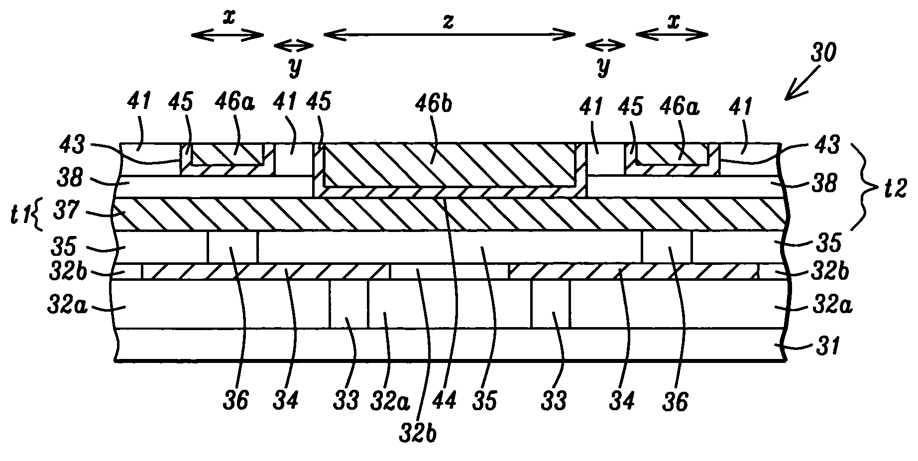
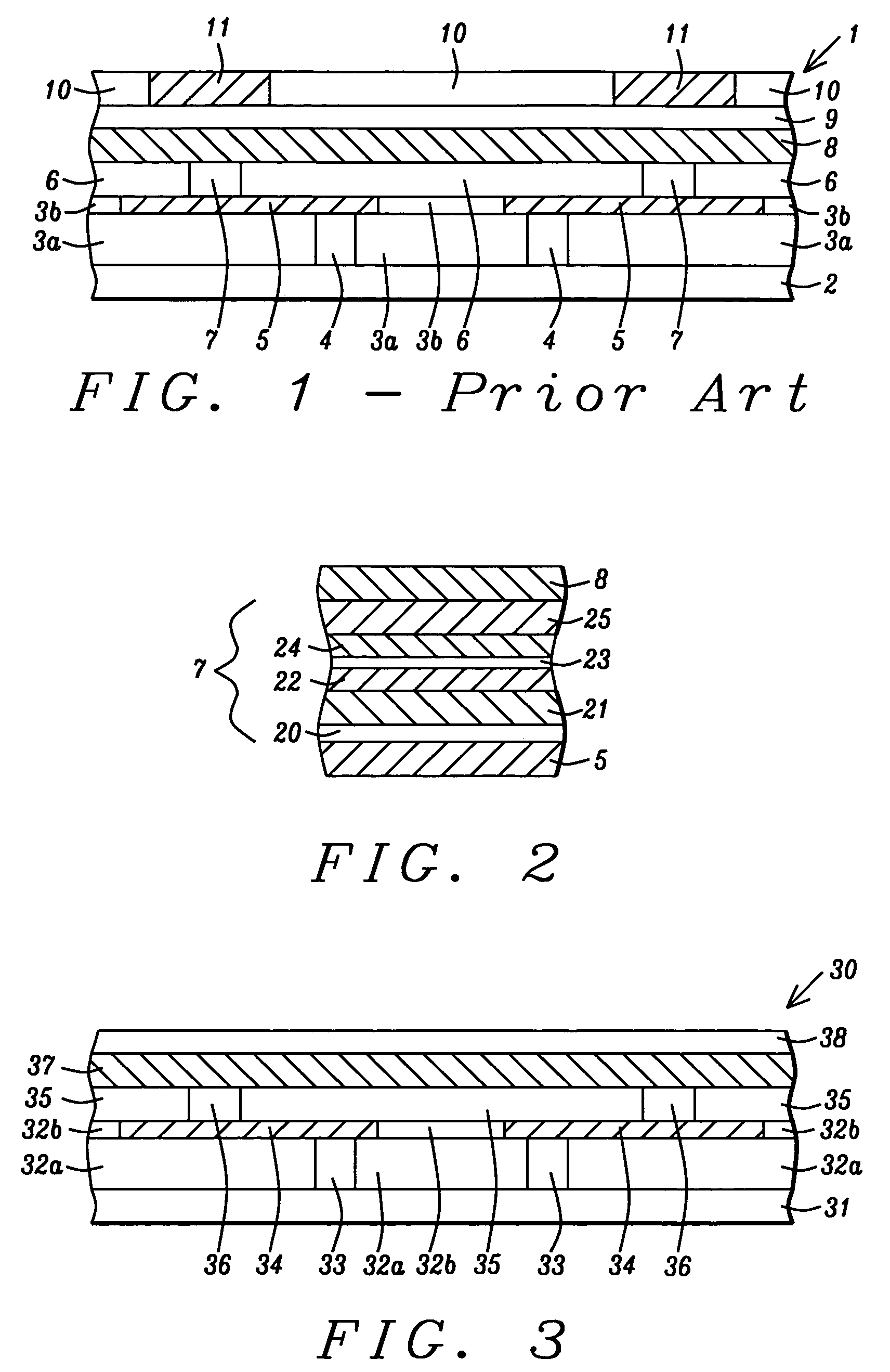
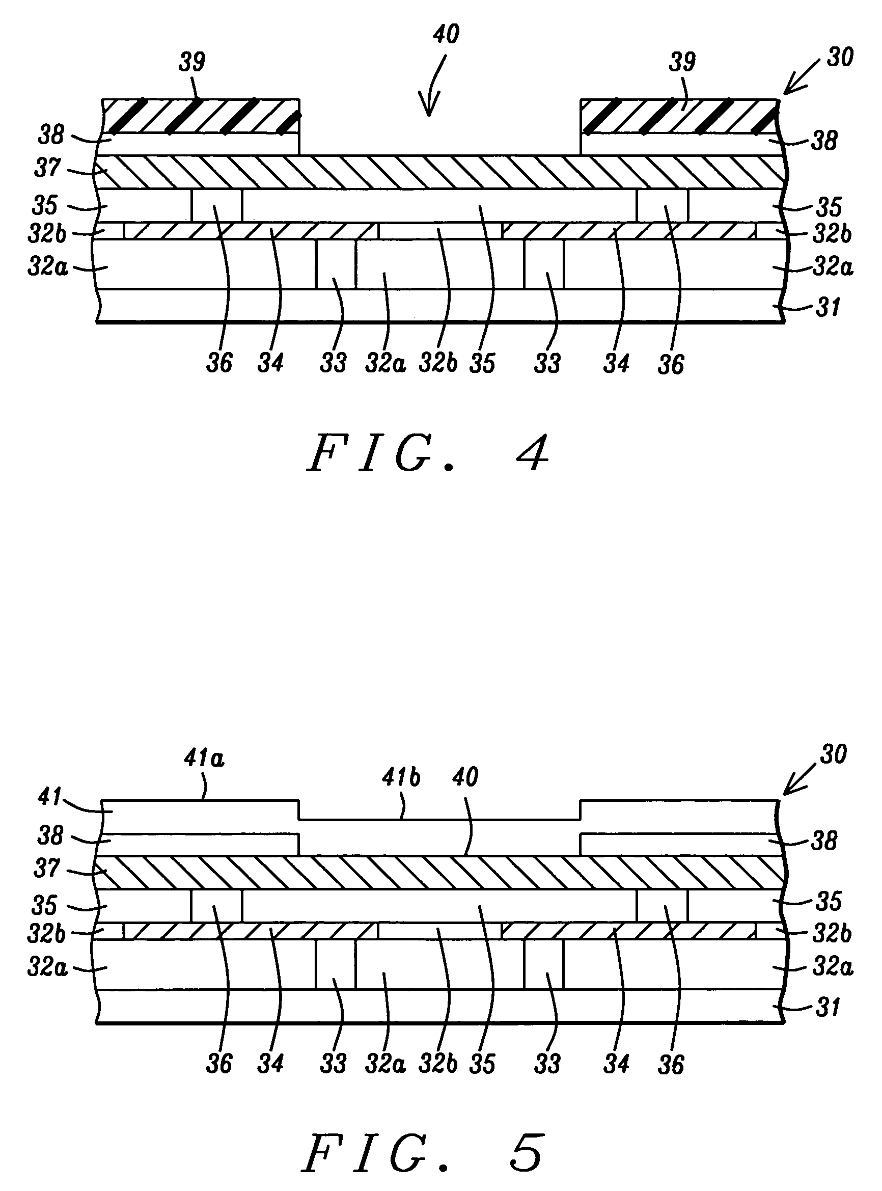
[0027]The present invention is an MRAM array on an MRAM chip in which bit lines formed above MTJs are thicker in certain regions in order to reduce bit line resistance. The drawings are provided by way of example and are not intended to limit the scope of the invention. Although only two MRAM cells are depicted in the cross-sectional views, it is understood that from a top-down view there are a plurality of MRAM cells in an array that includes multiple rows and multiple columns of cells on the MRAM chip. The MRAM array encompasses MTJs as well as nearby word lines and bit lines, and insulation layers between the conductive layers. Moreover, an MTJ may have a top spin valve or a bottom spin valve configuration. A method of forming the MRAM array of the present invention will be described first and is illustrated in FIGS. 3–8.

[0028]Referring to FIG. 3, a partially completed MRAM chip structure 30 is shown that includes a substrate 31 which may be silicon or another semiconductor subst...


PUM

PropertyMeasurementUnit
thicknessaaaaaaaaaa
thicknessaaaaaaaaaa
widthaaaaaaaaaa

Abstract

Improved MRAM arrays and a method of forming the same are disclosed in which a bit line has thinner portions formed over MTJs and thicker portions therebetween. Bottom electrodes are formed in a first insulation layer on a substrate and then MTJs and a coplanar second insulation layer are formed thereon. After a second conductive layer comprised of lower metal lines is formed above the MTJs, a trench is formed in a stack of insulation layers above portions of the lower metal lines. A barrier layer and upper metal layer are sequentially deposited and then planarized to form a filled trench that effectively increases a bit line thickness. The lower metal layer is a thin bit line in regions over MTJs. The method may also comprise forming word lines on an insulation layer that are aligned over the MTJs and perpendicular to the bit lines.

Description

FIELD OF THE INVENTION[0001]The invention relates to an MRAM structure, and more particularly, to an MRAM array in which the bit lines have a lower line resistance and are thicker in certain regions. The invention is also a method for fabricating the improved MRAM array.BACKGROUND OF THE INVENTION[0002]A magnetic random access memory (MRAM) chip is generally comprised of an array of parallel first conductive lines on a horizontal plane, an array of parallel second conductive lines on a second horizontal plane spaced above and formed in a direction perpendicular to the first conductive lines, and a magnetic tunnel junction (MTJ) formed at each location where a second conductive line crosses over a first conductive line. A first conductive line may be a word line while a second conductive line is a bit line or vice versa. Alternatively, a first conductive line may be a bottom electrode line while a second conductive line is a bit line (or word line). There may be an array of third con...

Claims


Application Information

Patent Timeline
Patent Type & Authority Patents(United States)
IPC IPC(8): H01L21/00H01L27/105G11C11/22H01L21/8246H01L27/22H01L43/08
CPCG11C7/18H01L27/222G11C11/16H10B61/00B21D28/34B21D28/28
Inventor WANG, PO-KANGHONG, LIUBO
Owner HEADWAY TECH INC
Why Eureka
Try Eureka