Methods for preserving strained semiconductor substrate layers during CMOS processing

a technology of semiconductor substrates and processing methods, applied in the field of semiconductor substrates, can solve the problems of increasing the complexity and functionality of semiconductor structures, new processing challenges, and limited processing windows for such structures, and achieves the effects of low processing cost, low cost, and high quality

Inactive Publication Date: 2006-07-04
TAIWAN SEMICON MFG CO LTD
View PDF18 Cites 28 Cited by
  • Summary
  • Abstract
  • Description
  • Claims
  • Application Information

AI Technical Summary

Benefits of technology

[0018]Accordingly, it is an object of the present invention to provide a method for forming a semiconductor structure having a strained semiconductor layer that overcomes the limitations of known methods. Specifically, in various embodiments of the invention, methods of providing dielectric layers, such as, for example, oxide layers, which avoid consuming unacceptably large amounts of the surface material in Si / SiGe heterostructure-based wafers are proposed to replace or supplement various intermediate CMOS thermal oxidation steps known in the art. First, by using oxide deposition methods such as chemical vapor deposition (CVD), arbitrarily thick dielectric layers may be formed with little or no consumption of surface silicon. These layers, for example, oxide layers, such as a screening oxide and pad oxide layers, are formed by deposition onto, rather than reaction with and consumption of the surface layer. Alternatively, oxide deposition is preceded by a thermal oxidation step of short duration, e.g., rapid thermal oxidation. Here, the short thermal oxidation consumes little surface Si, and the Si / oxide interface is of high quality. The oxide may then be thickened to a desired final thickness by deposition. Furthermore, the thin thermal oxide may act as a barrier layer to prevent contamination associated with subsequent oxide deposition.
[0022]In various embodiments, the method further includes introducing dopants into the semiconductor structure, wherein the screening layer affects the introduction of dopants into at least a portion of the structure by at least one of scattering dopants and reducing energy of the dopants. The method may also include subjecting the structure to a thermal anneal, wherein the screening layer hinders out-diffusion of the dopants from at least a portion of the substrate.
[0024]In general, in another aspect, a method for forming a structure includes forming a strained semiconductor layer over a substrate, depositing a pad oxide layer over at least a portion of a top surface of the strained semiconductor layer; and forming a masking layer over the pad oxide layer. The pad oxide layer substantially inhibits formation of stress-induced defects in the strained semiconductor layer. The masking layer may include silicon nitride.

Problems solved by technology

The increasing operating speeds and computing power of microelectronic devices have recently given rise to the need for an increase in the complexity and functionality of the semiconductor structures that are used as the starting substrates in these microelectronic devices.
However, because these devices are fabricated on Si / SiGe virtual substrates rather than on the Si substrates commonly utilized for complementary MOS (CMOS) technologies, they present new processing challenges.
For example, because thin, near-surface, strained heteroepitaxial layers constitute critical parts of devices formed on relaxed SiGe virtual substrates the processing windows for such structures are limited.
Traditional silicon-based CMOS process flows, therefore, may not be suitable for these layers because conventional CMOS processes typically result in the consumption of a large portion of surface substrate material.
This consumption is primarily due to thermal oxidation steps.
Accordingly, thermal oxidation is not desirable when processing wafers that incorporate thin surface layers formed on SiGe virtual substrates, where a final minimum thickness of 50 Å of the thin strained layer (from a starting thickness of, e.g., 50–200 Å) needs to be available for device channels.

Method used


Image

  • Methods for preserving strained semiconductor substrate layers during CMOS processing
  • Methods for preserving strained semiconductor substrate layers during CMOS processing
  • Methods for preserving strained semiconductor substrate layers during CMOS processing

Examples


Embodiment Construction

[0033]In accordance with various embodiments of the present invention, layers deposited on semiconductor substrates replace traditionally grown layers, thereby reducing the consumption of substrate surface material. Various features of the invention are well suited to applications utilizing MOS devices that include, for example, Si, Si1−xGex, and / or Ge layers in and / or on a substrate. The term “MOS” is used herein to refer generally to semiconductor devices that include a conductive gate spaced at least by an insulating layer from a semiconducting channel layer. The terms “SiGe,”“Si1−xGex,” and “Si1−yGey” refer to silicon-germanium alloys.

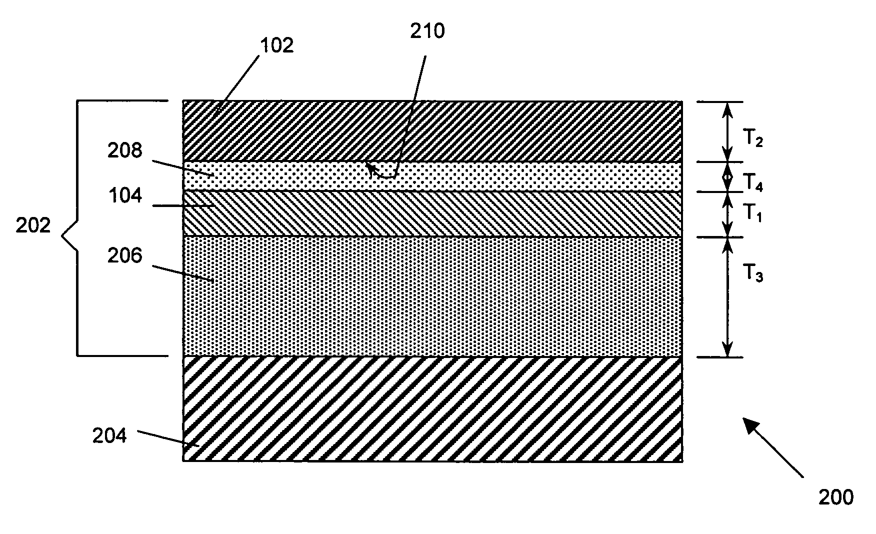
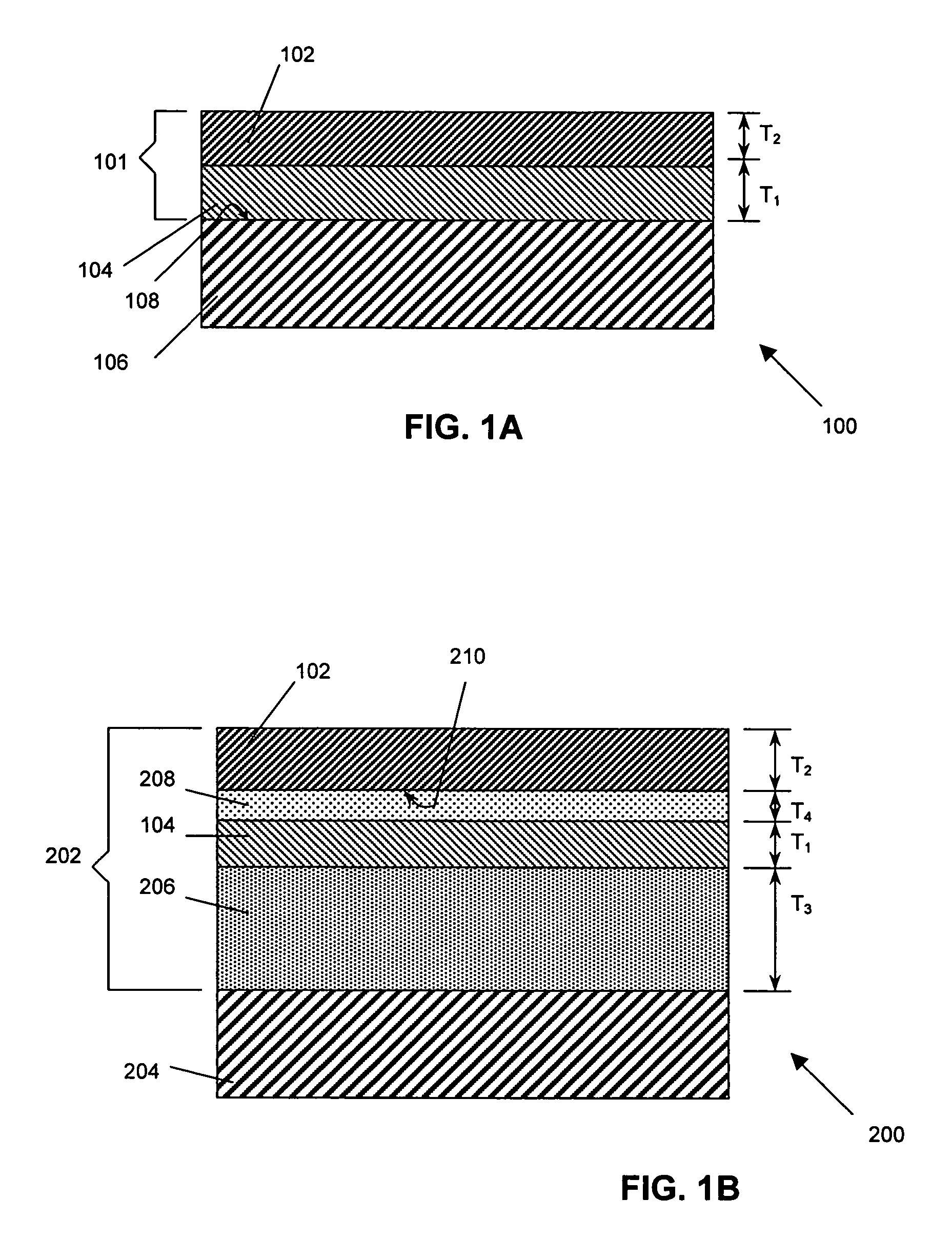
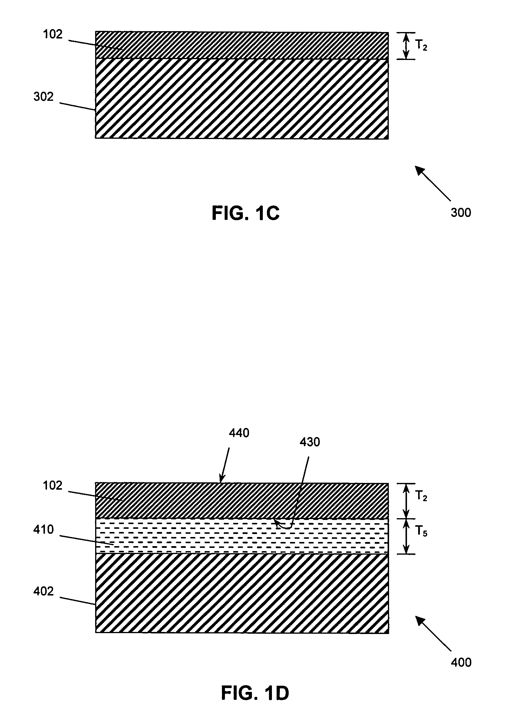
[0034]Referring to FIG. 1A, which illustrates an epitaxial wafer 100 suitable to use with the present invention, several layers collectively indicated at 101, including a strained layer 102 and a relaxed layer 104, are disposed over a substrate 106. The substrate 106 comprises a semiconductor, such as silicon, silicon deposited over an insulator, s...


PUM

PropertyMeasurementUnit
thicknessaaaaaaaaaa
surface roughnessaaaaaaaaaa

Abstract

Oxidation methods, which avoid consuming undesirably large amounts of surface material in Si / SiGe heterostructure-based wafers, replace various intermediate CMOS thermal oxidation steps. First, by using oxide deposition methods, arbitrarily thick oxides may be formed with little or no consumption of surface silicon. These oxides, such as screening oxide and pad oxide, are formed by deposition onto, rather than reaction with and consumption of the surface layer. Alternatively, oxide deposition is preceded by a thermal oxidation step of short duration, e.g., rapid thermal oxidation. Here, the short thermal oxidation consumes little surface Si, and the Si / oxide interface is of high quality. The oxide may then be thickened to a desired final thickness by deposition. Furthermore, the thin thermal oxide may act as a barrier layer to prevent contamination associated with subsequent oxide deposition.

Description

CROSS-REFERENCE TO RELATED APPLICATION[0001]This application claims the benefit of and priority to U.S. Provisional Application Ser. No. 60 / 422,468, filed on Oct. 30, 2002, the disclosure of which is incorporated herein by reference.FIELD OF THE INVENTION[0002]This invention relates generally to semiconductor substrates and specifically to formation of dielectric layers on semiconductor substrates.BACKGROUND OF THE INVENTION[0003]The increasing operating speeds and computing power of microelectronic devices have recently given rise to the need for an increase in the complexity and functionality of the semiconductor structures that are used as the starting substrates in these microelectronic devices. Such “virtual substrates” based on silicon and germanium provide a platform for new generations of very large scale integration (“VLSI”) devices that exhibit enhanced performance when compared to devices fabricated on bulk Si substrates. Specifically, new technological advances enable fo...

Claims


Application Information

Patent Timeline
Patent Type & Authority Patents(United States)
IPC IPC(8): H01L21/00H01L21/44H01L21/46H01L21/48H01L21/50H01L21/20H01L21/265
CPCH01L21/0237H01L21/02381H01L21/0245H01L21/0251H01L29/1054H01L21/02664H01L21/2652H01L21/02532H01L21/02521H01L21/02538H01L21/823807
Inventor CURRIE, MATTHEW T.LOCHTEFELD, ANTHONY J.
Owner TAIWAN SEMICON MFG CO LTD
Why Eureka
Try Eureka