Electron-beam-addressed active-matrix spatial light modulator

Inactive Publication Date: 2006-07-11
VIDEO DISPLAY CORP
View PDF14 Cites 12 Cited by
  • Summary
  • Abstract
  • Description
  • Claims
  • Application Information

AI Technical Summary

Benefits of technology

[0027]Each selected transistor is subsequently enabled in a writing manner that results in the polarization direction of the specified light being selectively rotated in the corresponding liquid-crystal cell. When there are multiple selected transistors, all of the selected transistors are enabled substantially simultaneously in the writing manner. This results in the polarization directions of the specified light being selectively rotated substantially simultaneously in all of the liquid-crystal cells corresponding to the selected transistors. Using a suitably located polarization analyzer, the combination of the liquid-crystal cells, substrate, and polarization analyzer thereby presents the entire image at substantially the same instant. Operating in this manner enables the active-matrix light modulator of the invention to avoid undesirable time-varying image artifacts.
[0031]Spacer elements are preferably situated between the liquid-crystal cells. The spacer elements provide substantially uniform liquid-crystal cell thickness. This avoids image gray-scale non-uniformities due to changes in optical path length of the modulated light.
[0033]The present active-matrix light modulator operates in a highly efficient manner. In addition to avoiding undesirable image artifacts, the modulator's spatial resolution is largely not limited by parasitic impedances of addressing electrodes. The image is highly uniform. The operating life is long due to the elimination of liquid-crystal degradation caused by residual DC voltage across image-carrying cells of prior electron-beam-addressed light modulators.

Problems solved by technology

The performance of the Eidophor and Talaria light-valve oil-film projection systems was satisfactory but, even with continuous exhaust, the maintenance and operating cost of the systems was high.
However, the construction methods and substrate materials fundamentally limited the display resolution.
Additionally, an unfavorable aspect ratio resulting from the large substrate thickness compared to the diameter of the feedthrough pins generated capacitive crosstalk between pins.
This further reduced display resolution.
This resulted in unwanted residual DC voltage on the liquid crystal.
Commercialization opportunities for the Tektronix display were also limited by the difficulty involved with fabrication of the liquid-crystal cells in a high-vacuum environment.
In each case of recent prior art where the addressing technique utilizes charge deposition by an electron beam and where the display technique employs liquid-crystal modulation resulting from the deposited charge, the mechanism used to transfer information (electrical signals) from the electron-beam target to the display electrodes of the liquid crystal cells has fundamentally limited the resolution of the display.
Variations in the spacing distance produce optical path differences, leading to non-uniform image gray level and corresponding loss in image quality.
Although flexibility of the substrates enhances conformal properties, a lack of flatness when the modulator is used in reflective mode can result in reflected image distortion.
The overlapping row activation, as well as the typically slow optical response of liquid-crystal material, creates undesirable artifacts in time-varying images.
These bus electrodes degrade image quality due to resistive losses in each bus electrode between its driver and its pixel TFTs and due to capacitive coupling between each bus electrode and other pixel TFTs in proximity to that bus electrode.
These parasitic capacitances reduce the spatial resolution in conventional AMLCDs because, as the pixel TFTs become smaller, the fixed parasitic capacitances become a larger fraction of the total pixel capacitances.

Method used


Image

  • Electron-beam-addressed active-matrix spatial light modulator
  • Electron-beam-addressed active-matrix spatial light modulator
  • Electron-beam-addressed active-matrix spatial light modulator

Examples


Embodiment Construction

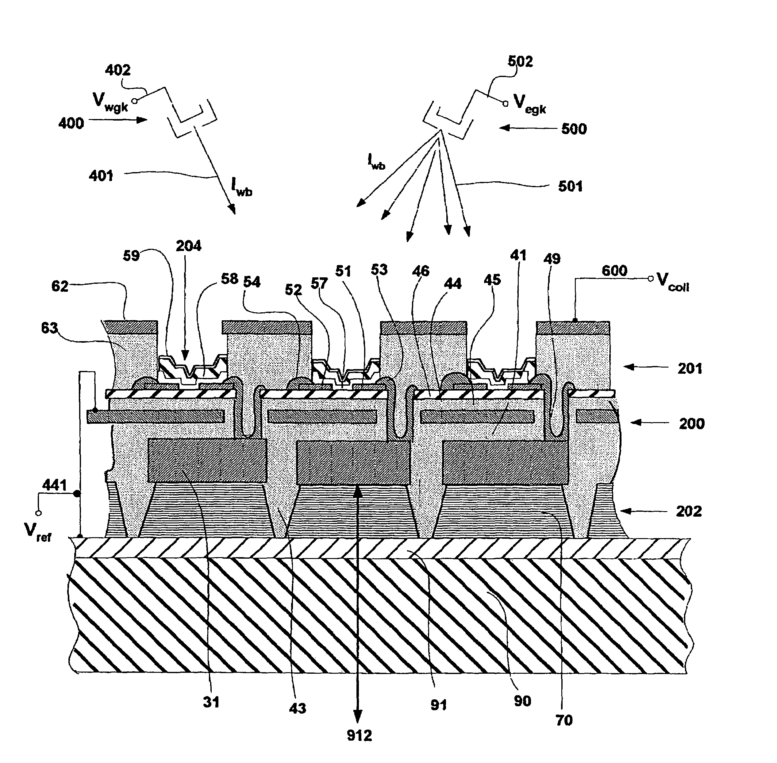
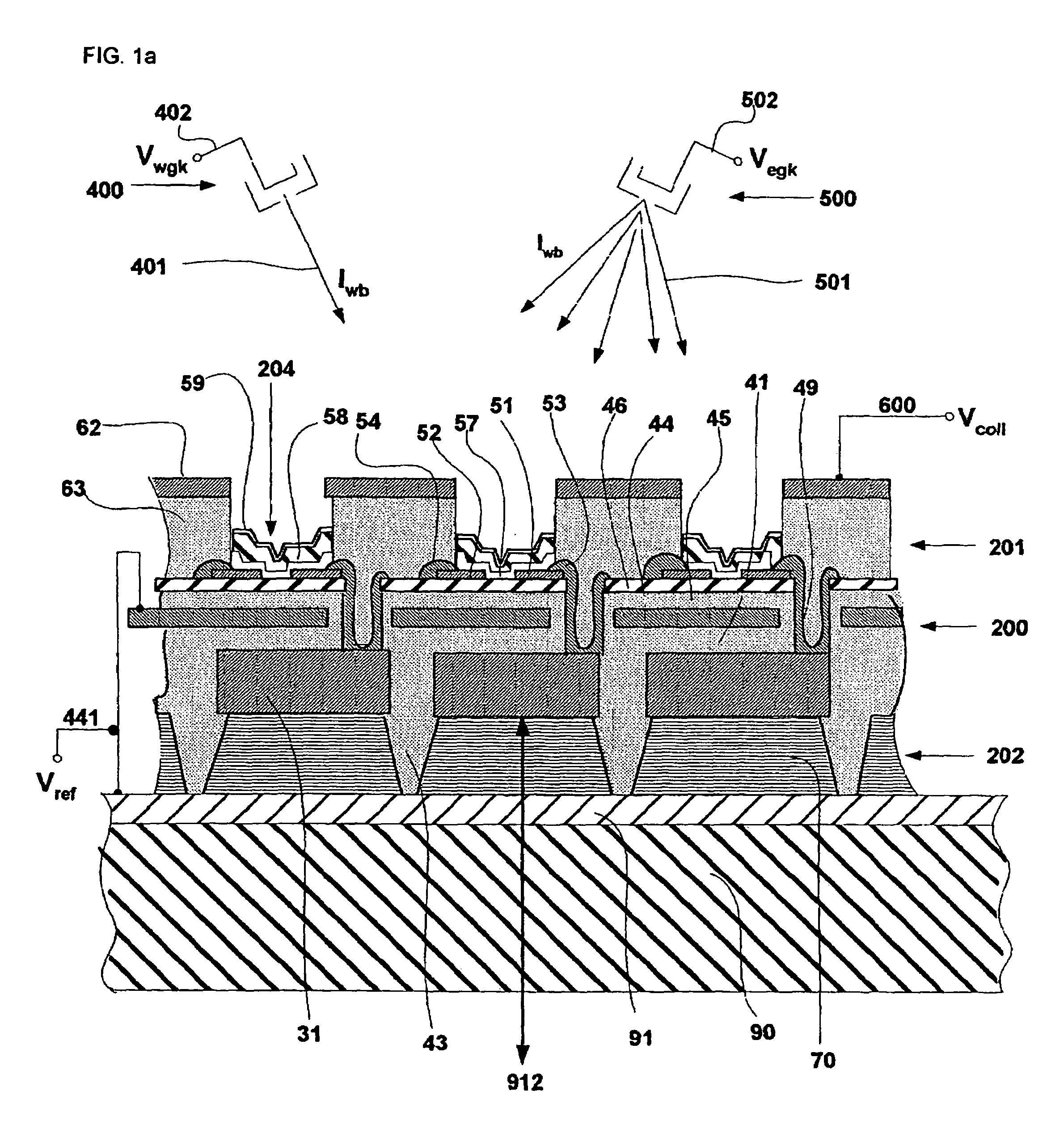
[0057]The present invention furnishes a reflective liquid-crystal light modulator addressed by an array of thin-film transistors, wherein each display element has electrical and mechanical isolation from adjacent and proximate display elements. Image information is provided to the active array by means of a scanning electron beam.

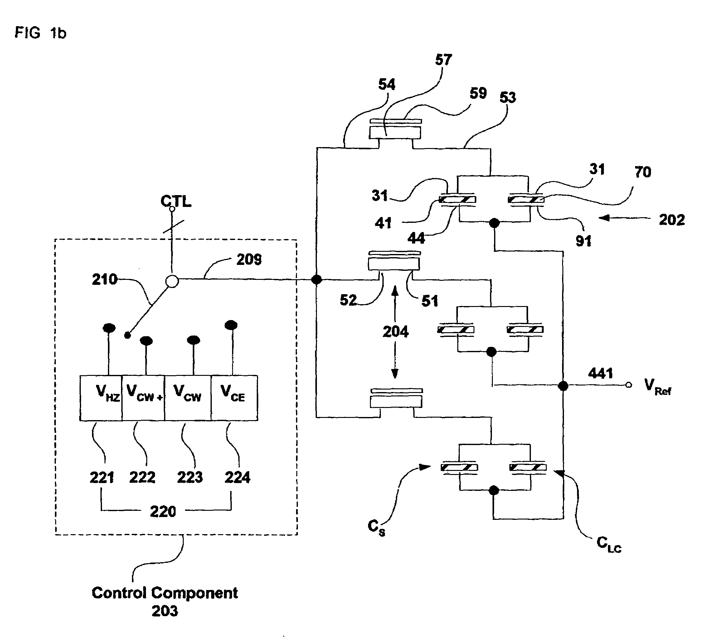
[0058]Referring to the drawings, FIGS. 1a and 1b (collectively “FIG. 1”) together illustrate a reflective liquid-crystal light modulator in accordance with the invention. The light modulator of FIG. 1 includes a thin flexible membrane 200, an active matrix 201 disposed along one side (the upper side in FIG. 1a) of membrane 200, a two-dimensional array of display electrodes 31 disposed along the other side (the lower side in FIG. 1a) of membrane 200, electrically conductive means 49 for electrical communication between active matrix 201 and display electrodes 31, a layer 70 of liquid crystal divided into a two-dimensional array of liquid-crystal cells 202 re...


PUM


Abstract

A spatial light modulator contains a substrate (90), a plurality of overlying liquid-crystal cells (202), a plurality of respectively corresponding transistors (204), an electron-beam system (400 and 500), and a control component (203). Each transistor is in electrical communication with the corresponding liquid-crystal cell. The electron-beam system bombards each transistor with electrons that cause it to be selectively in (i) a non-conductive condition in which its channel-region electric field is substantially insufficient for conduction or (ii) a conductive condition in which its channel-region electric field is sufficient for at least partial conduction. During selected time periods when a transistor is in its conductive condition, the control component provides the transistor with a control signal that results in the polarization direction of specified light being selectively rotated in passing through the corresponding liquid-crystal cell.

Description

CROSS-REFERENCE TO RELATED APPLICATION[0001]This application claims the priority of, and hereby incorporates by reference, U.S. provisional patent application 60 / 457,444, filed 26 Mar. 2003.FIELD OF USE[0002]This invention relates to image presentation and, more particularly, to liquid-crystal image presentation technology.BACKGROUND OF THE INVENTION[0003]As computer-generated image technology becomes more realistic, the need for projection display systems capable of reproducing images with high fidelity becomes critical. High-fidelity projection display systems are needed in electronic entertainment applications, and are essential in simulation and training where the perceived reality of the environment is central to the purpose of the simulation and training.[0004]An essential feature of image fidelity is the property of image resolution. It is desirable for the spatial resolution of the display to be higher than the resolution of the addressing means so that image quality is not ...

Claims


Application Information

Patent Timeline
IPC IPC(8): G02F1/133G09G3/02G09G3/36G09G5/00
CPCG02F1/133348G02F1/1362G09G3/3648G09G3/36G09G3/02
Inventor VIDAL, MARCIALMUTCHLER, DAVID K.HAVEN, DUANE A.
Owner VIDEO DISPLAY CORP
Why Eureka
Try Eureka