Semiconductor integrated device and apparatus for designing the same

a technology of integrated devices and semiconductors, applied in the direction of emergency protective arrangements, pulse techniques, instruments, etc., can solve the problem of difficult to manufacture lsi with sufficient esd tolerance, and achieve the effect of suppressing the influence of esd current and reducing wiring resistan

Active Publication Date: 2006-07-11
RENESAS ELECTRONICS CORP
View PDF15 Cites 19 Cited by
  • Summary
  • Abstract
  • Description
  • Claims
  • Application Information

AI Technical Summary

Benefits of technology

[0015]wherein the first ground wiring is coupled to the second ground wiring, and the second interface circuit unit is placed in the vicinity of the first interface circuit unit. By adopting this configuration, it is possible to reduce the wiring resistance and thereby to suppress an influence of an ESD current.

Problems solved by technology

In particular, as miniaturization of an LSI progresses, the ESD designing in consideration of the miniaturization requires many processes at design and development stages.
Accordingly, this prior art causes variation of ESD tolerance and it is therefore difficult to manufacture an LSI with sufficient ESD tolerance.

Method used


Image

  • Semiconductor integrated device and apparatus for designing the same
  • Semiconductor integrated device and apparatus for designing the same
  • Semiconductor integrated device and apparatus for designing the same

Examples


first embodiment

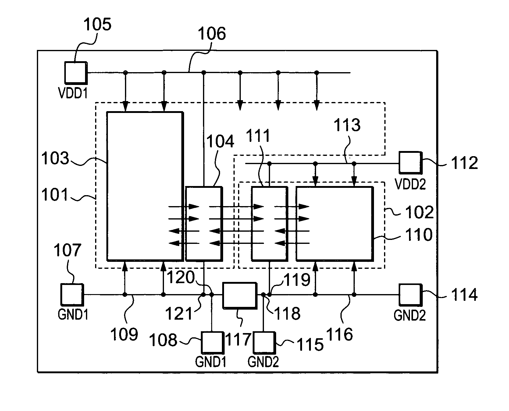
[0032]FIG. 1 is a block diagram for describing a schematic circuit configuration of an LSI device according to a first embodiment. With reference to FIG. 1, the LSI device of the first embodiment includes a first power system circuit unit 101 which is operated by electric power supplied from a first power system, and a second power system circuit unit 102 which is operated by electric power supplied from a second power system.

[0033]Typical examples of the first power system circuit unit and the second power system circuit unit are a digital circuit unit and an analog circuit unit to be placed in an LSI chip. Other examples may include an LSI device configured to use different power systems between a digital internal circuit and an input / output interface circuit unit.

[0034]Moreover, the digital circuit unit, for instance, has a larger number of elements than the analog circuit unit, and the digital circuit unit, also, has a larger chip area than the analog circuit unit.

[0035]In a hyb...

second embodiment

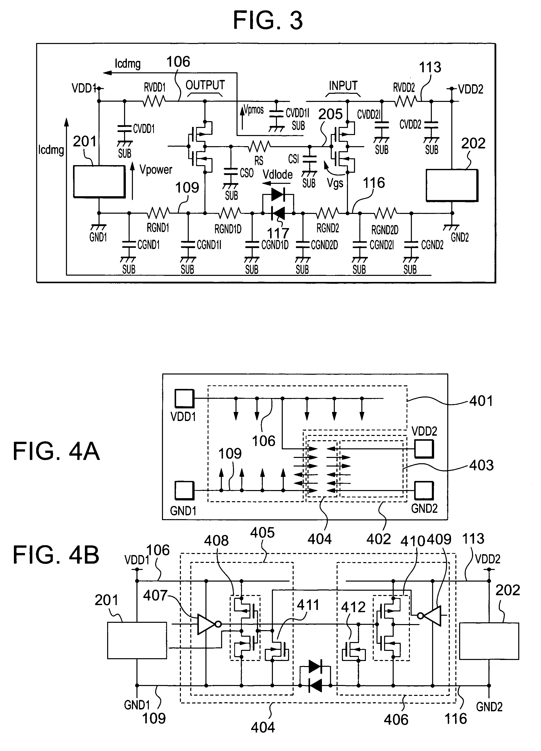
[0072]FIG. 4A is a circuit diagram showing a schematic configuration of an LSI according to a second embodiment of the present invention. The LSI of this embodiment includes a digital circuit as a first power system circuit, and an analog circuit as a second power system circuit. Part of the analog circuit is designed as an analog macro, and the analog macro contains a first power system input / output circuit to be operated by a first power supply.

[0073]In FIG. 4A, the LSI of this embodiment includes a digital circuit unit 401 and an analog macro 402. The analog macro 402 includes an analog internal circuit 403 and an input / output circuit unit 404.

[0074]FIG. 4B is a circuit diagram showing a detailed configuration of the input / output circuit unit 404 of the analog macro. The input / output circuit unit 404 includes a first power system input / output circuit unit 405 and a second power system input / output circuit unit 406. In FIG. 4B, the input / output circuit unit 404 of the analog macro...

third embodiment

[0080]Next, a third embodiment according to the present invention will be described with reference to FIG. 5. FIG. 5 is a circuit diagram showing a schematic configuration of an LSI device of this embodiment. As described in FIG. 5, the LSI device of this embodiment includes a protection element 501 between VDD1 and GND1 which is coupled between the first power system power supply wiring 106 and the first power system ground wiring 109, and a protection element 502 between VDD2 and GND2 which is coupled between the second power system power supply wiring 113 and the second power system ground wiring 116.

[0081]In general, the power supply protection element clamps the electric potential between the power supply and the ground to the clamp potential upon application of the ESD if the potential difference between the power supply and the ground reaches or exceeds the clamp potential. Various widely known elements, such as a clamp element applying a transistor, can be used as the protec...


PUM

PropertyMeasurementUnit
voltage Vgsaaaaaaaaaa
voltageaaaaaaaaaa

Abstract

A semiconductor integrated device includes a plurality of power system circuit units, a first circuit unit 101 to which electric power is supplied from first power supply wiring 106, and first ground wiring 109 to which the first circuit unit is coupled. Moreover, the semiconductor integrated device includes a second circuit unit 102 to which electric power is supplied from second power supply wiring 113, and second ground wiring 116 coupled to the second circuit unit.
The first circuit unit includes a first interface circuit unit 104, and the second circuit unit includes a second interface circuit unit 111 configured to perform inputting or outputting of a signal to and from the first interface circuit unit. The first ground wiring is coupled to the second ground wiring through a protection circuit 117, and the second interface circuit unit is placed in the vicinity of the first interface circuit unit.

Description

BACKGROUND OF THE INVENTION[0001]1. Field of the Invention[0002]The present invention relates to a semiconductor integrated device and an apparatus for designing the same, more specifically, to a semiconductor integrated device including a plurality of circuits to be operated by a plurality of power supplies and an apparatus for designing the same.[0003]2. Description of the Prior Art[0004]Along with an increase in cell density of a semiconductor integrated device (hereinafter abbreviated as an “LSI”) and advance in the digital technology in recent years, circuits including digital circuits and analog circuits in single LSI chips are embedded in many products. In a digital camera or video equipment, for example, a DA converter and an AD converter for converting signals between analog signals and digital signals are embedded as a single chip.[0005]Each of the digital circuit and the analog circuit embedded in the single chip is operated by a plurality of different power systems. More...

Claims


Application Information

Patent Timeline
Patent Type & Authority Patents(United States)
IPC IPC(8): G06F17/50H01L27/04H01L21/82H01L23/528H01L23/60H01L27/02H03K19/00H03L5/00
CPCG06F17/505H01L23/60G06F2217/78H01L23/5286H01L27/0251H01L2224/16145H01L2224/48091H01L2924/13091H01L2224/48227H01L2924/00014H01L2924/00G06F30/327G06F2119/06D06M11/00D06M15/564D06M2200/12D10B2401/021D10B2501/04
Inventor HIRATA, MORIHISA
Owner RENESAS ELECTRONICS CORP
Why Eureka
Try Eureka